Flash memory cell and fabrication thereof
a technology of flash memory and cell, which is applied in the direction of semiconductor devices, electrical devices, transistors, etc., can solve the problems of difficult to increase the area between the control gate and the floating gate, and raise so as to achieve the effect of raising the gate coupling ratio (gcr) of the cell
- Summary
- Abstract
- Description
- Claims
- Application Information
AI Technical Summary
Benefits of technology
Problems solved by technology
Method used
Image

Examples
first embodiment
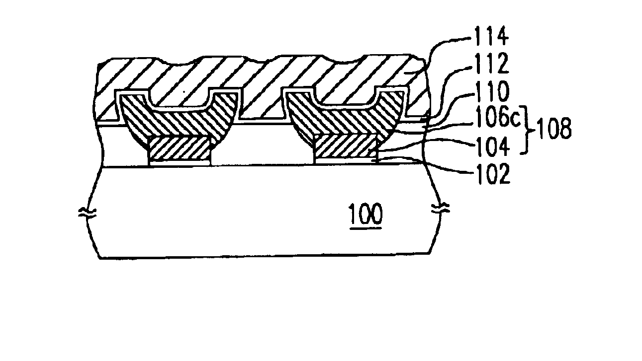
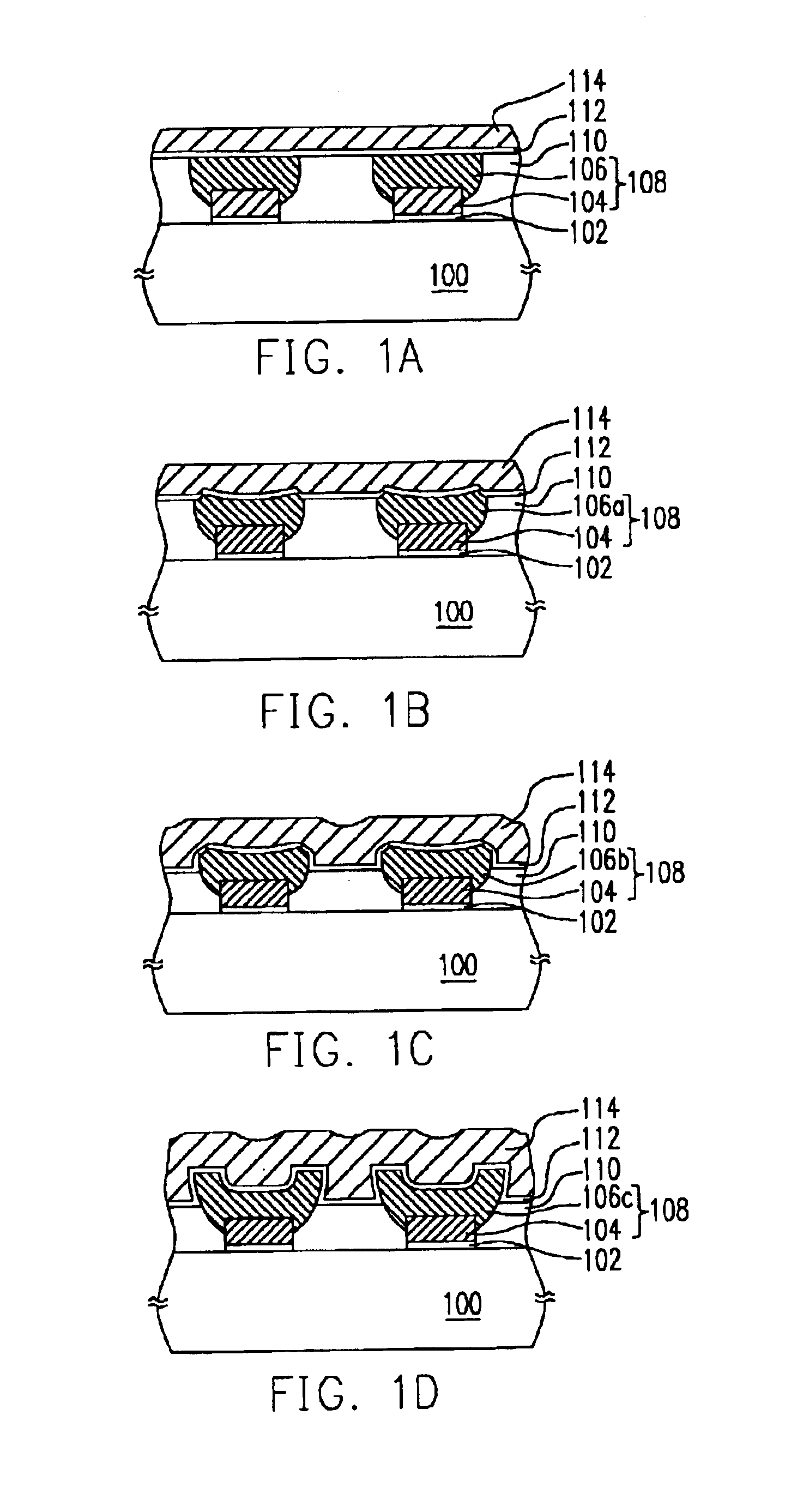
[0022]FIGS. 1A-1D illustrate some structural variations of a flash memory cell according to the first preferred embodiment of this invention in a cross-sectional view, wherein the common constituents in the four drawings are labeled with the same reference numbers and described only once.
[0023]Referring to FIG. 1A, the flash memory cell of this invention includes a substrate 100, a tunnel oxide layer 102, two conductive layers 104 and 106, an insulating layer 110, an inter-gate dielectric layer 112 and a conductive layer 114.
[0024]The conductive layer 104 is disposed on the substrate 100 with the tunnel oxide layer 102 between them, and the conductive layer 106 is disposed on the conductive layer 104 contacting with the latter. The two conductive layers 106 and 104 together constitute a floating gate 108, wherein the conductive layer 106 may have a bowl-like cross section. The insulating layer 110 fills up the gaps between the floating gates 108, and the control gate 114 is disposed...
second embodiment
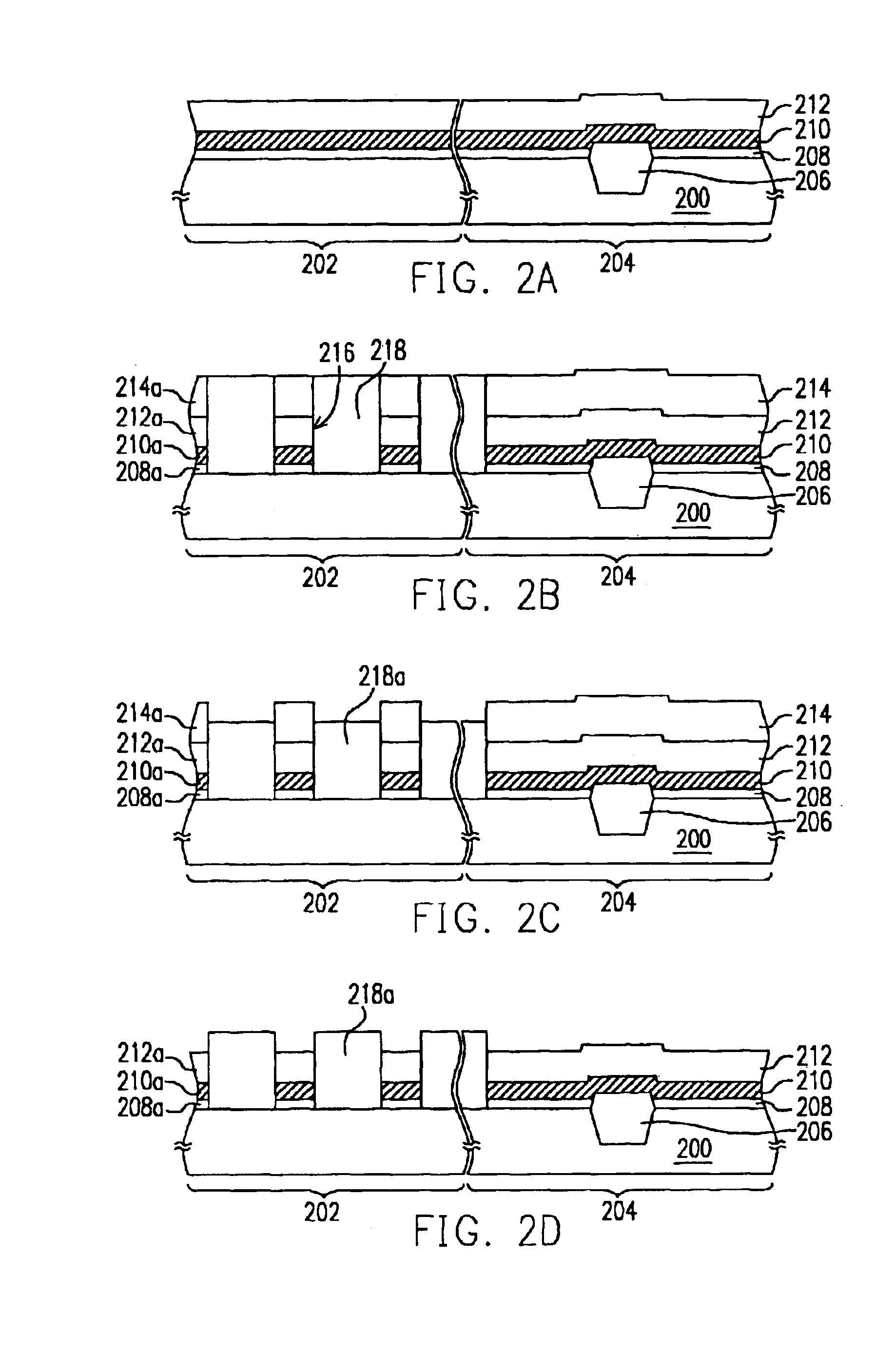
[0027]FIGS. 2A-2H illustrate a process flow of fabricating a flash memory device according to the second embodiment of this invention in a cross-sectional view. The second embodiment of this invention is described in detail referring to FIGS. 2A-2H.
[0028]Referring to FIG. 2A, a substrate 200 like a silicon substrate is provided, which is divided into a memory area 202 and a periphery circuit area 204. Device isolation 206 is formed in the periphery circuit area 204 with a local oxidation (LOCOS) process or a shallow trench isolation (STI) process to define active areas.
[0029]Referring to FIG. 2A again, a tunnel oxide layer 208, a conductive layer 210 and an insulating layer 212 are sequentially formed on the substrate 200. The tunnel oxide layer 208 is constituted of a material such as silicon oxide, and is formed with a method such as thermal oxidation or low-pressure chemical vapor deposition (LPCVD). The material of the conductive layer 210 is doped polysilicon, for example, whic...
third embodiment
[0042]FIGS. 3A-3D illustrate a process flow of fabricating a flash memory device according to the third embodiment of this invention in a cross-sectional view. The third embodiment of this invention is described in detail referring to FIGS. 3A-3D, wherein the constituents that have been illustrated in FIGS. 2A-2H are labeled with the same reference numbers, and are not described again.
[0043]Referring to FIG. 3A, a substrate 200 like a silicon substrate is provided, which is divided into a memory area 202 and a periphery circuit area 204. The above-mentioned processes that correspond to FIGS. 2A-2E in the second embodiment are sequentially performed to form a device isolation 206, a tunnel oxide layer 208 / 208a, a conductive layer 210 / 210a, an insulating layer 218b and an opening 220 having a bowl-like cross-section.
[0044]Referring to FIG. 3B, a conductive layer 222 is formed on the substrate 200 without fully filling up the openings 220. The conductive layer 222 is constituted of a m...
PUM
 Abstract
Description
Claims
Application Information
 - R&D
- Intellectual Property
- Life Sciences
- Materials
- Tech Scout
- Unparalleled Data Quality
- Higher Quality Content
- 60% Fewer Hallucinations
Browse by: Latest US Patents, China's latest patents, Technical Efficacy Thesaurus, Application Domain, Technology Topic, Popular Technical Reports.
© 2025 PatSnap. All rights reserved.Legal|Privacy policy|Modern Slavery Act Transparency Statement|Sitemap|About US| Contact US: help@patsnap.com