Method and system for placing logic nodes based on an estimated wiring congestion

a logic node and wiring congestion technology, applied in the field of methods and systems for placing logic nodes based on estimated wiring congestion, can solve the problems of overload and failure, the placement of logic nodes on a chip is especially problematic, and the wiring interconnects between logic nodes cannot be placed arbitrarily close to each other, so as to avoid overload and failure

Inactive Publication Date: 2005-06-07
GLOBALFOUNDRIES INC
View PDF22 Cites 14 Cited by
  • Summary
  • Abstract
  • Description
  • Claims
  • Application Information

AI Technical Summary

Problems solved by technology

Moreover, the wiring interconnects between the logic nodes cannot be placed arbitrarily close to each other.
Placement of nodes on a chip is especially problematic when the wiring requirements between the logic nodes approaches the wiring availability.
In these situations, the resulting wiring congestion can cause “hot spots” on the chip, which can lead to overload and failure thereof.
Although this allows the logic nodes to be physically positioned on the chip, it does not guarantee a wireable chip placement.
In the case of the former, several time-consuming iterations are required.
In the case of the latter, increasing the chip size will led to a substantial increase in cost.

Method used


Image

  • Method and system for placing logic nodes based on an estimated wiring congestion
  • Method and system for placing logic nodes based on an estimated wiring congestion
  • Method and system for placing logic nodes based on an estimated wiring congestion

Examples


Embodiment Construction

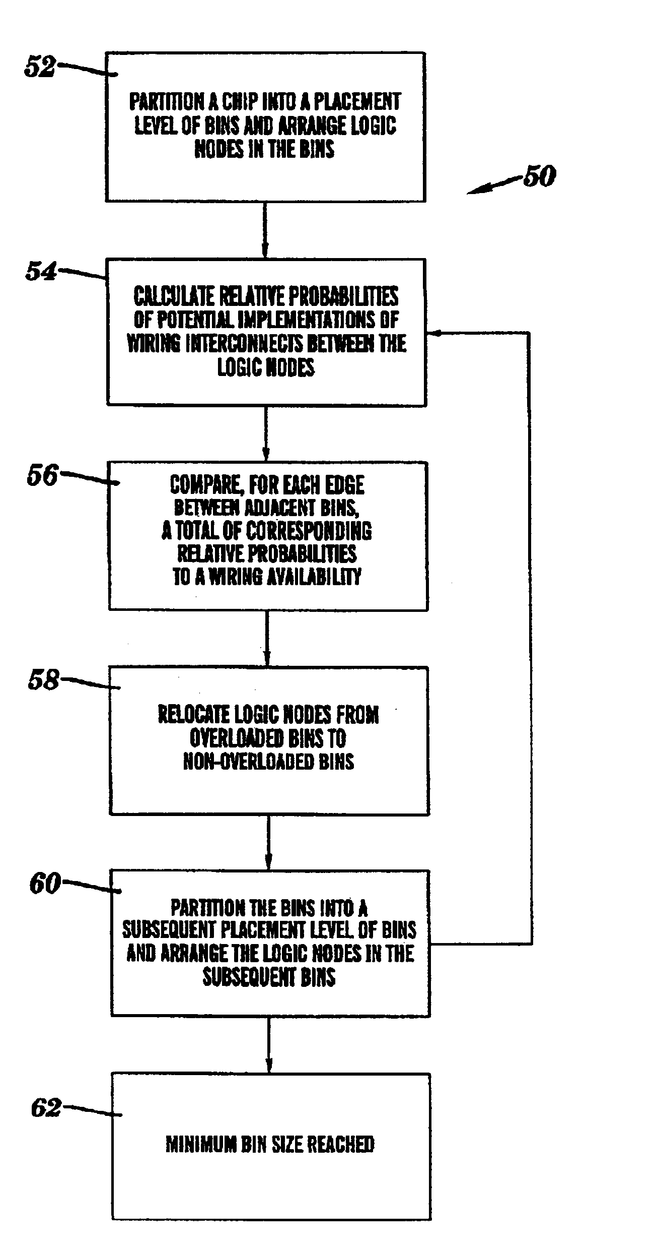
[0023]In general, the present invention provides a method and system for placing logic nodes based on an estimated wiring congestion. This allows the logic nodes to be placed within wiring constraints in an efficient manner. As indicated above, previous methods fail to provide such a capability.

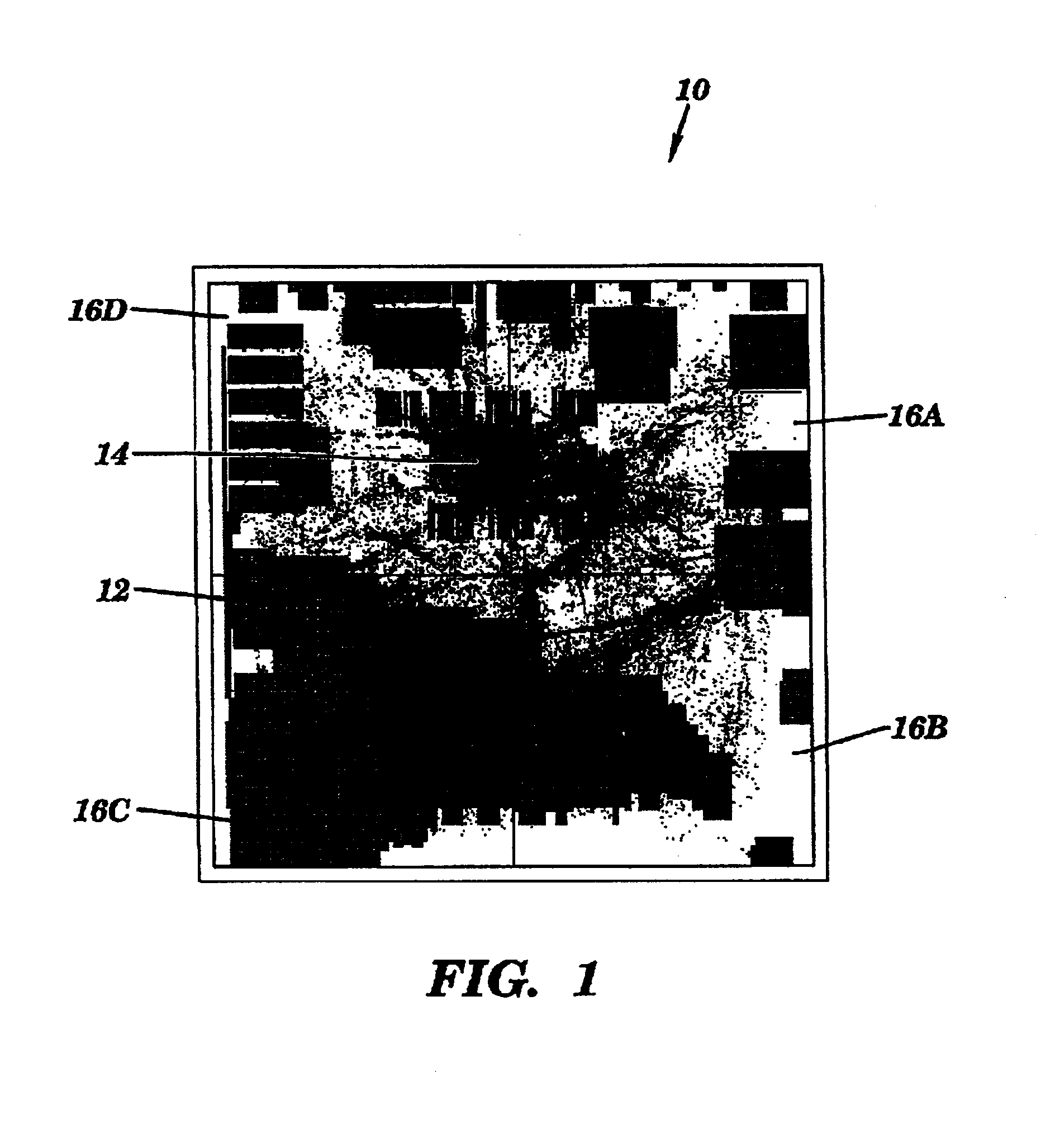
[0024]Referring now to FIG. 1, a chip 10 having logic nodes 12 and 14 according to the present invention is shown. Logic nodes 12 and 14 typically include circuits, transistors and other nodes known to be placed on a chip 10. As indicated above, previous methods for placing logic on a chip were primarily concerned with geographically fitting the logic. Generally, this included positioning the logic on a chip, partitioning the chip into four bins or quadrants, and then arranging the logic in an overlapping manner in the four bins. In general, the positioning and arranging of the logic nodes was accomplished via quadratic optimization, min-cut or other known operation. In the case of the former...


PUM


Abstract

A method and system for placing logic nodes based on an estimated wiring congestion are provided. Specifically, under the present invention, relative probabilities for potential implementations of wiring interconnects between logic nodes are determined. Then, for each edge between adjacent bins, a total of corresponding relative probabilities is compared to a wiring availability. Based on the comparison, the logic nodes can be placed within wiring constraints.

Description

BACKGROUND OF THE INVENTION[0001]1. Field of the Invention[0002]The present invention generally provides a method and system for placing logic nodes based on an estimated wiring congestion. Specifically, the present invention provides a method and system for placing logic nodes into bins of a chip based on a comparison of an estimated wiring congestion to a wiring availability.[0003]2. Background Art[0004]In the manufacture of microelectronics, circuits and other logic must be placed on chips under certain wireability and timing constraints. Specifically, the nodes must be placed so that the wiring interconnects between the nodes are within the wiring constraints of the chip. Moreover, the wiring interconnects between the logic nodes cannot be placed arbitrarily close to each other. Rather, a certain wiring pitch must be observed. Placement of nodes on a chip is especially problematic when the wiring requirements between the logic nodes approaches the wiring availability. In these s...

Claims


Application Information

Patent Timeline
Patent Type & Authority Patents(United States)
IPC IPC(8): G06F17/50
CPCG06F17/5072G06F30/392
Inventor BRENNER, ULRICHHONSINGER, PHILIP S.KOEHL, JUERGENKORTE, BERNHARDROHE, ANDREVYGEN, JENS P.
Owner GLOBALFOUNDRIES INC
Why Eureka
Try Eureka