
System and method for placement of dummy metal fills while preserving device matching and/or limiting capacitance increase

a technology of dummy metal fills and capacitance increases, applied in cad circuit design, program control, instruments, etc., can solve the problems of increasing the capacitance of the original metal line, affecting the electrical field, and complex integrated circuit devices with high complexity and circuit density. achieve the effect of limiting the capacitance increas

Inactive Publication Date: 2005-06-07
MAGMA DESIGN AUTOMATION
View PDF6 Cites 76 Cited by
  • Summary
  • Abstract
  • Description
  • Claims
  • Application Information

AI Technical Summary

Benefits of technology

"The present invention relates to systems and methods for placing dummy metal fills in an integrated circuit fabrication process while preserving device matching and limiting capacitance increase. The invention takes into account the influence of dummy metal fills that are transferred to structures printed on the wafer and can result in disturbance of device matching and increased capacitance. The invention includes a computer-automated method for locating dummy fills in an integrated circuit layout and designating critical nets and metal conductors. The method includes steps to delineate a net blocking exclusion zone around metal conductors to prevent disturbance of device matching. The invention also includes a system for locating dummy fills and a computer-automated method for designating critical nets and metal conductors. The technical effects of the invention include improved accuracy in locating dummy fills and minimizing capacitance increase, which can enhance the performance and functionality of integrated circuits."

Problems solved by technology

Thus, one of the critical steps in the fabrication process is the formation of interconnects that connect the layers of the integrated circuit device, resulting in integrated circuit devices with high complexity and circuit density.
However, one problem with the rule-based dummy fill is that the range of allowable dummy-filled density is relatively large such that the prescribed density is generally determined through trial-and-error for each design.
However, the inserted dummy metal fills adversely affect the electrical field and increase the capacitance of the original metal lines.
Some nets span across the entire chip making their effect on the performance of the chip critical.
Thus, a 25% net delay increase can be sufficient to cause a fault condition for the circuit functionality.
However, it is difficult to reduce the capacitance increase for all nets and the method proposed by Tian can not guarantee a reduction of the capacitance increase to within a specified range for the long timing-critical nets.
The inserted dummy metal fills may also adversely affect other characteristics of the original circuit or device design.

Method used


Image

  • System and method for placement of dummy metal fills while preserving device matching and/or limiting capacitance increase
  • System and method for placement of dummy metal fills while preserving device matching and/or limiting capacitance increase
  • System and method for placement of dummy metal fills while preserving device matching and/or limiting capacitance increase

Examples


Embodiment Construction

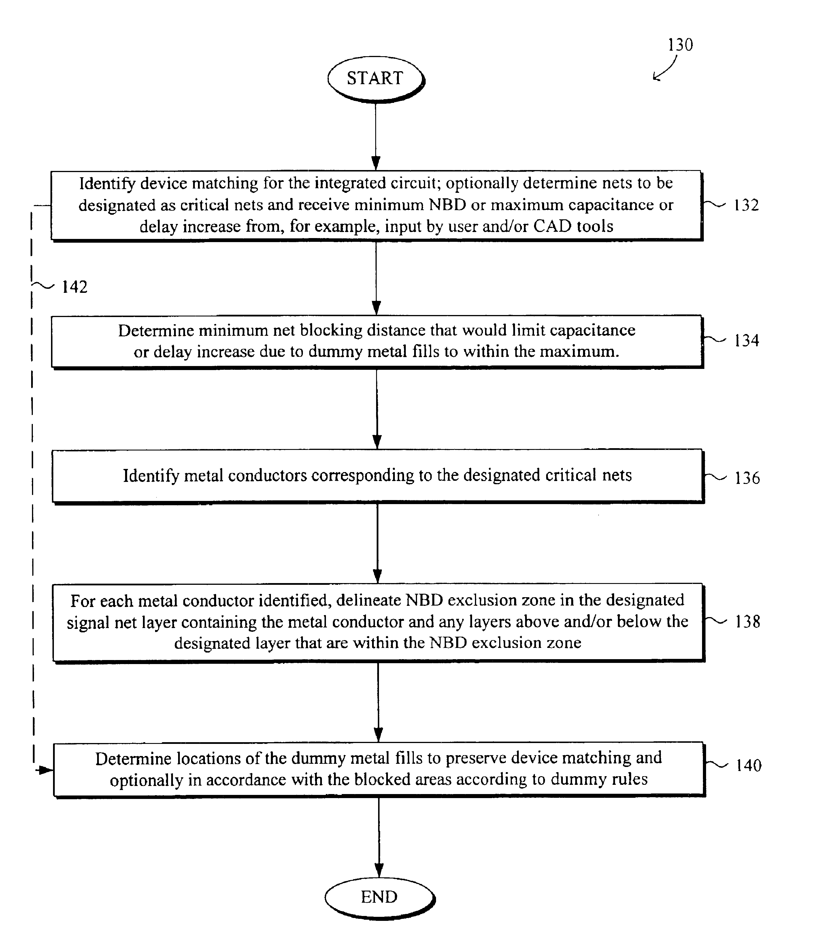
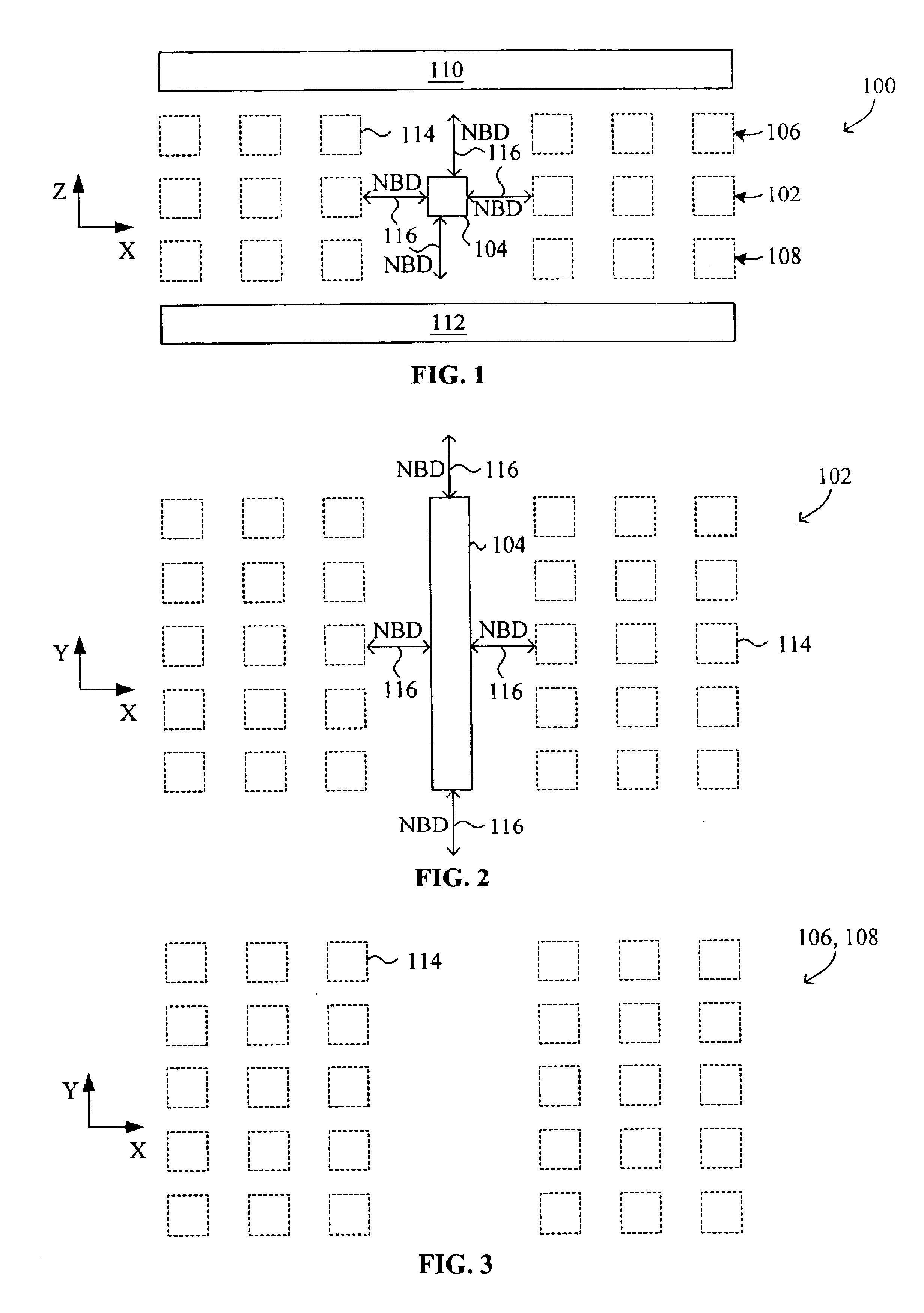
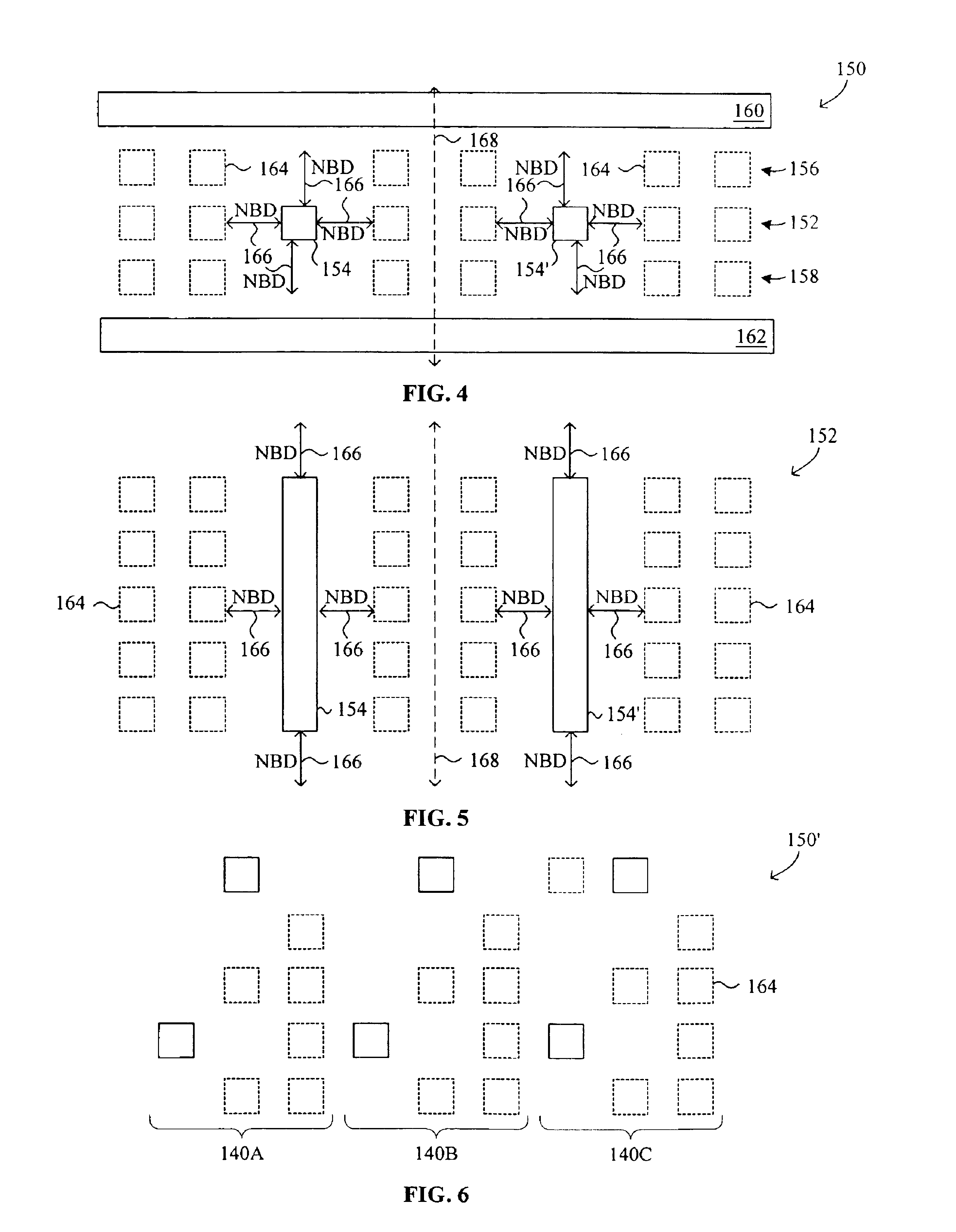
[0035]Systems and methods for placement of dummy metal fills while preventing disturbance of device matching and optionally limiting capacitance increase are disclosed. The following description is presented to enable any person skilled in the art to make and use the invention. Descriptions of specific embodiments and applications are provided only as examples and various modifications will be readily apparent to those skilled in the art. The general principles defined herein may be applied to other embodiments and applications without departing from the spirit and scope of the invention. Thus, the present invention is to be accorded the widest scope encompassing numerous alternatives, modifications and equivalents consistent with the principles and features disclosed herein. For purpose of clarity, details relating to technical material that is known in the technical fields related to the invention have not been described in detail so as not to unnecessarily obscure the present inv...


PUM


Abstract

Systems and methods for placement of dummy metal fills while preventing disturbance of device matching and optionally limiting capacitance increase are disclosed. A computer-automated method for locating dummy fills in an integrated circuit fabrication process generally comprises receiving an input layout of the integrated circuit and specification of device matching for the integrated circuit and locating the dummy fills in the integrated circuit according to dummy rules while preserving device matching. Locating the dummy fills may include locating the dummy fills along the at least one axis of symmetry where device matching is along an axis of symmetry and locating the dummy fills so as to preserve matching of the repeated elements where device matching is repeated matched elements. The method may also include designating at least one net of the integrated circuit as a critical net, the critical nets being only a subset of all nets of the integrated circuit, identifying metal conductors corresponding to each designated critical net from the layout file, and delineating a net blocking exclusion zone extending a distance of a minimum net blocking distance (NBD) from the metal conductor for each metal conductor identified, wherein the step of locating locates the dummy fills outside of the net blocking exclusion zone.

Description

CROSS REFERENCE TO RELATED APPLICATIONS[0001]This application is a continuation-in-part of co-pending U.S. patent application Ser. No. 10 / 097,978 entitled “System And Method For Limiting Increase In Capacitance Due To Dummy Metal Fills Utilized For Improving Planar Profile Uniformity,” filed on Mar. 12, 2002, the entirety of which is incorporated herein by reference.BACKGROUND OF THE INVENTION[0002]1. Field of the Invention[0003]The present invention relates generally to semiconductor processing. More specifically, systems and methods for placement of dummy metal fills while preventing disturbance of device matching and optionally limiting capacitance increase are disclosed.[0004]2. Description of Related Art[0005]Typically, an integrated circuit fabrication process involves a series of layering processes in which metallization, dielectrics, and other materials are applied to the surface of a semiconductor wafer to form a layered interconnected structure. The integrated circuits for...

Claims


Application Information

Patent Timeline
Patent Type & Authority Patents(United States)
IPC IPC(8): G06F17/50
CPCG06F30/39
Inventor OH, SOO-YOUNG
Owner MAGMA DESIGN AUTOMATION
Learn More