
Touch panel and electronic apparatus using the same

a technology of electronic equipment and touch panel, which is applied in the field of touch panel, can solve the problems of displaying yellowish color and impairing the evaluation of the apparatus, and achieve the effects of low cost, low yellowish color, and minimal change in display color

Inactive Publication Date: 2005-06-07
PANASONIC CORP
View PDF8 Cites 20 Cited by
  • Summary
  • Abstract
  • Description
  • Claims
  • Application Information

AI Technical Summary

Benefits of technology

"The present invention provides a transparent panel (TP) that includes a first transparent substrate with a first transparent conductive layer and a second transparent substrate with a second transparent conductive layer. The second conductive layer opposes the first conductive layer with a certain clearance. The TP has a b* value of 2.0 or smaller in the L*a*b* color specification. The first and second substrates can also have a layer for color adjustment that generates optical interference. The TP can also contain a colorant that has a complementary color to the conductive layer. The TP is less yellowish and shows minimal change in display color when attached on a color display device. When attached on a display surface of a liquid crystal display device or the like of an electronic apparatus, the electronic apparatus shows a high quality color display along with a minimal sense of incompatibility."

Problems solved by technology

Since the transparent conductive layers 2 and 5, made of ITO, SnO2or the like, have a slightly yellowish color, conventional TPs sometimes exhibit a yellowish color, which is one of the problems of the TPs.
This impairs evaluation of the apparatus, and requests for improvement have been increasingly arising.

Method used


Image

  • Touch panel and electronic apparatus using the same
  • Touch panel and electronic apparatus using the same
  • Touch panel and electronic apparatus using the same

Examples


first exemplary embodiment

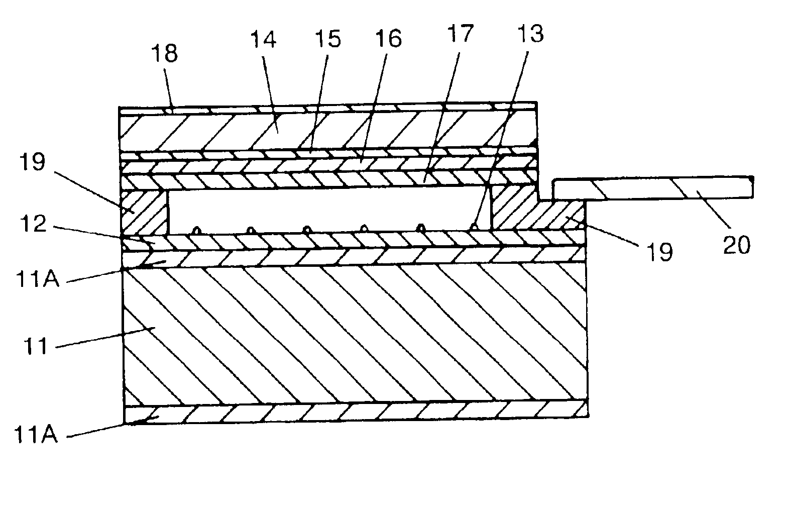
[0028]FIG. 1 shows a cross sectional view of a TP in accordance with a first exemplary embodiment of the present invention. A first transparent substrate 11, or a lower substrate, is made of 1.1 mm thick soda lime glass.

[0029]The first transparent substrate 11 is provided at both of an upper and a lower surfaces with silicon dioxide (SiO2) layers 11A for preventing alkaline substance from dissolving out of the glass material. On the upper SiO2 layer 11A, a first transparent conductive layer 12 of ITO having a refractive index of 1.9 is formed at a thickness of 200 Å.

[0030]The light transmittance of the transparent substrate 11 including the upper and the lower SiO2layers 11A and the transparent conductive layer 12 is measured using a visible light spectrophotometer. The transmitted light does not have a peak spectrum at a specific wavelength; the total luminous transmittance in accordance with JIS K 7361-1 (hereinafter referred to as total transmittance) is 94%, and b* value specifi...

second embodiment

[0067]FIG. 5 is a cross sectional view of a TP in accordance with a second exemplary embodiment of the present invention. Referring to FIG. 5, a first transparent conductive layer 32 made of an ITO and having a refractive index of 1.9 is formed on an upper surface a first transparent substrate 31 made of 1.1 mm thick soda lime glass.

[0068]Spectral transmittance through the transparent substrate 31 including the first transparent conductive layer 32 formed thereon, does not show a peak, total transmittance is 90%, and the b* value is 2.0.

[0069]The transparent substrate 31 in the present embodiment is also provided with SiO2 layers for preventing alkaline substance from dissolving out of the glass. Illustration and description of the SiO2 layers are omitted here.

[0070]Very small sized dot spacers 33 made of an insulating epoxy resin or similar material are provided on a surface of the transparent conductive layer 32 and are disposed at a specific pitch.

[0071]A second transparent subst...

third embodiment

[0084]FIG. 6 is a cross sectional view of a TP in accordance with a third exemplary embodiment of the present invention. Referring to FIG. 6, a first transparent substrate 41 of a biaxially oriented PET film is supported at the lower surface, via an adhesive layer 42 made of an acrylic resin, by a transparent supporting substrate 43 of a 1.0 mm thick polycarbonate sheet.

[0085]An ITO layer 44 of refractive index of 1.9, and an SiO2 layer 45 of a refractive index of 1.4, are formed on an upper surface of the transparent substrate 41. The ITO layer 44 and the SiO2 layer 45 are formed at a predetermined thickness to function as a color adjustment layer.

[0086]A first transparent conductive layer 46 of an ITO having a refractive index of 1.9 is provided on an upper surface of the SiO2 layer 45.

[0087]Spectral transmittance through the transparent substrate 41, the color adjustment layer consisting of the ITO layer 44 and the SiO2 layer 45, the transparent conductive layer 46, the transpare...


PUM

PropertyMeasurementUnit
wavelengthaaaaaaaaaa
thickaaaaaaaaaa
refractive indexaaaaaaaaaa

Abstract

A touch panel has a first transparent substrate with a first transparent conductive layer, and a second transparent substrate with a second transparent conductive layer. Color of the touch panel has a b* value of 2.0 or smaller with respect to the L*a*b* color specification in accordance with JIS Z 8729. At least one of the first and second transparent substrates is provided with a color adjustment layer providing optical interference. The touch panel may further have a third transparent substrate provided with a color adjustment layer, or a third transparent substrate containing a colorant having color complementary to a color of the transparent conductive layer. The touch panel has a less yellowish appearance, and shows minimal color change of a color display device. When attached on a liquid crystal display device in an electronic apparatus, the electronic apparatus exhibits a high grade color display without a sense of incompatibility.

Description

FIELD OF THE INVENTION[0001]The present invention relates to a touch panel which is attached in front of a display surface of a liquid crystal display device or similar display devices. The touch panel makes it possible to input a certain specific signal corresponding to contents displayed on the display device by pressing its surface with a pen or a finger. The present invention also relates to an electronic apparatus using the touch panel.BACKGROUND OF THE INVENTION[0002]An increasing number of electronic apparatus have been employing a touch panel (hereinafter the touch panel is referred to as TP), which enables the input of a certain specific signal corresponding to displayed contents by pressing the relevant place on the display screen with a pen or a finger. In the following, a conventional TP is described referring to the drawings. The drawings used in the present invention are shown expanded in the direction of panel thickness for the sake of easier understanding.[0003]FIG. ...

Claims


Application Information

Patent Timeline
Patent Type & Authority Patents(United States)
IPC IPC(8): G06F3/033G02F1/1333G06F3/041G06F3/045G06F3/048H01H13/02H01H13/712
CPCG02F1/13338G06F3/0488G06F3/045G02F2001/133521G02F1/133521
Inventor NAKANISHI, AKIRAYAMAUE, NOBUHIROFUJII, SHIGEYUKI
Owner PANASONIC CORP
Learn More