Negative feedback amplifier with electrostatic discharge protection circuit

Active Publication Date: 2005-05-31
NEOPHOTONICS CORP
View PDF5 Cites 17 Cited by
  • Summary
  • Abstract
  • Description
  • Claims
  • Application Information

AI Technical Summary

Benefits of technology

[0017]An object of the present invention is to provide a negative feedback amplifier in which an amplifier is effectively protected from ESD with small reduction in a band width fw.
[0019]According to the present invention the following effect can be obtained due to the configuration of the negative feedback amplifier as described above.

Problems solved by technology

A transistor for amplification positioned in an input section especially sustains the damage from ESD.
Since the electric current increases the temperature of the junction, the resistance thereof decreases and causes overheating.
Then, the junction is damaged by melting.
However, there is a problem that the capacitance of the diodes 4 and 5, connected between the input terminal of the amplifiers 1 and the power terminals 2 and 3, adversely affects high-frequency characteristics.
The conventional electrostatic protective circuit, however, has the following problem.
Thus, it is difficult to obtain the desired band width fw.

Method used


Image

  • Negative feedback amplifier with electrostatic discharge protection circuit
  • Negative feedback amplifier with electrostatic discharge protection circuit
  • Negative feedback amplifier with electrostatic discharge protection circuit

Examples


first embodiment

(First Embodiment)

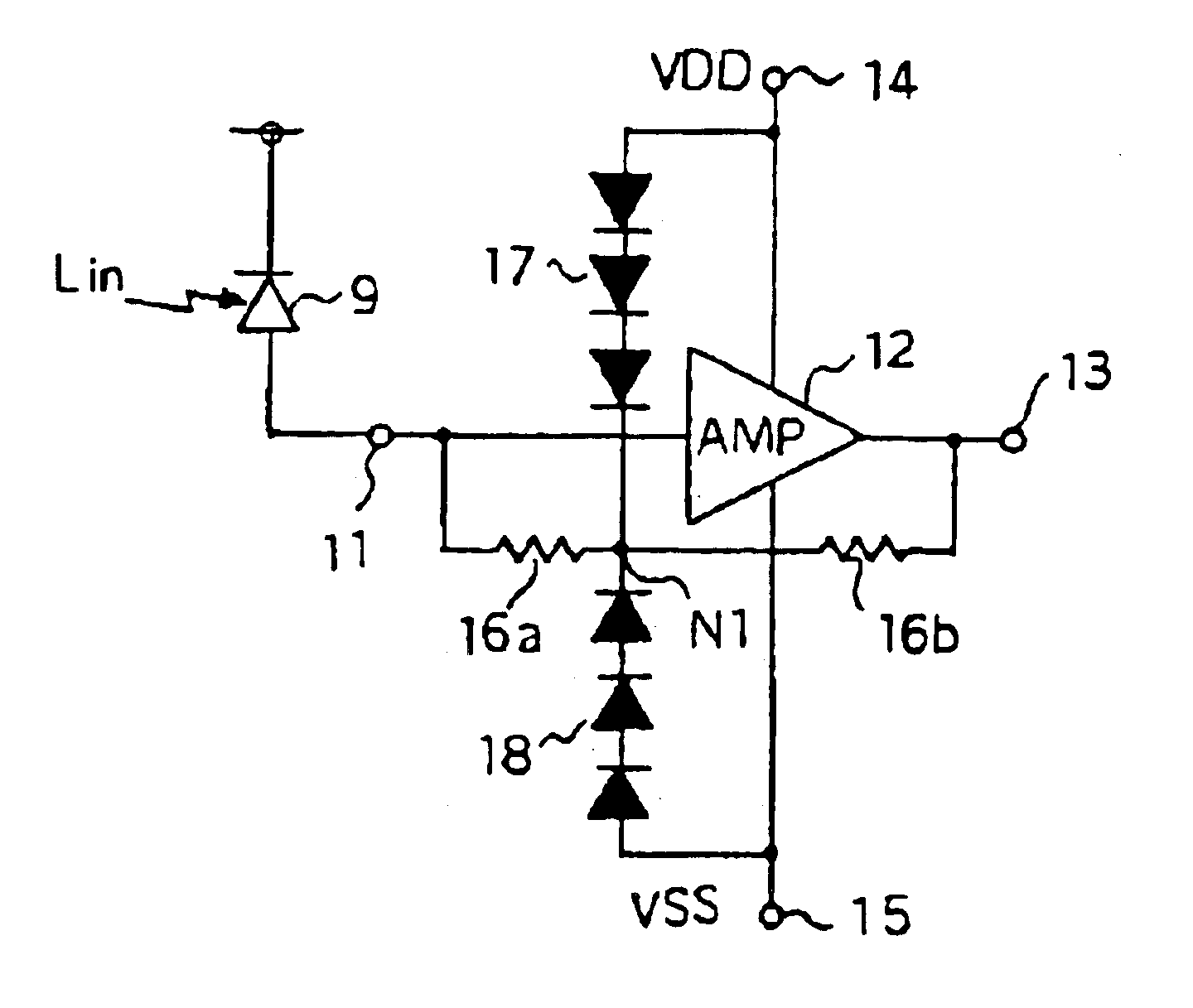
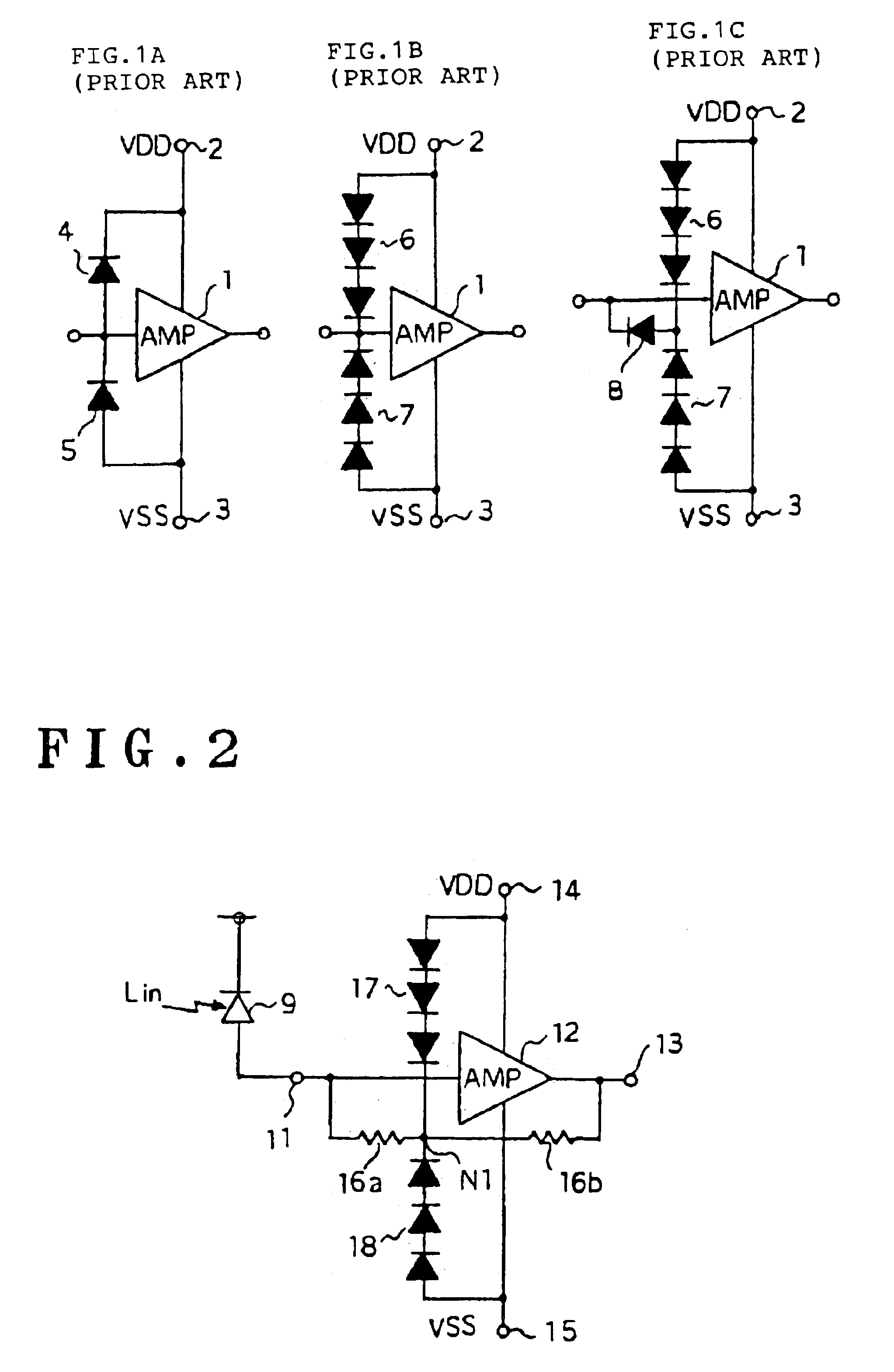
[0028]FIG. 2 is a schematic circuit diagram of a negative feedback amplifier according to a first embodiment of the present invention.

[0029]The negative feedback amplifier is an amplifier for use in a high-speed optical fiber communication system or the like, and which converts optical signals into electronic signals and amplifies the electronic signals. The negative feedback amplifier has an input terminal 11 into which current signals are inputted from a photoelectric conversion element 9 such as a photodiode, the conductivity of which varies in accordance with the intensity of the optical signals Lin. The input terminal 11 is connected to an amplifier (AMP) 12 which is to be protected and is composed of HEMTs. The output of the amplifier 12 is connected to an output terminal 13. Power supply voltages VDD and VSS are applied to the amplifier 12 from a positive power terminal 14 and a negative power terminal 15, respectively.

[0030]A feedback resistor comprising re...

second embodiment

(Second Embodiment)

[0041]FIG. 4 is a schematic circuit diagram of a negative feedback amplifier according to a second embodiment of the present invention. The same reference numerals are assigned to the same elements of FIG. 4 as those of FIG. 2.

[0042]The negative feedback amplifier is provided with protective diodes 19 and 20, in addition to the protective diodes 17 and 18 shown in FIG. 2. The protective diodes 19 and 20 are opposite in polarity to the protective diodes 17 and 18. The anodes of the diodes 19 and 20 are connected to the node N1. The cathodes of the diodes 19 and 20 are connected to the positive power terminal 14 and the negative power terminal 15, respectively. The diodes 19 and 20, just as with the diodes 17 and 18, comprise a plurality of Schottky diodes connected in series, in such a manner as to become to be in an off-state when the normal input signals are inputted. In the Schottky diode, the source and the drain of the HEMT, formed in the same process as the a...

third embodiment

(Third Embodiment)

[0046]FIG. 5 is a schematic circuit diagram of a negative feedback amplifier according to a third embodiment of the present invention. The same reference numerals are assigned to the same elements of FIG. 5 as those of FIG. 2.

[0047]The negative feedback amplifier is provided with protective diodes 17A, 18A and 21, instead of the protective diodes 17 and 18 shown in FIG. 2. The protective diodes 17A, 18A, and 21 have slightly different configuration from the protective diodes 17 and 18. The cathodes of the diodes 17A and 18A are connected to the node N2. The anodes of the diodes 17A and 18A are connected to the positive power terminal 14 and the negative power terminal 15, respectively. The anode of the diode 21 is connected to the node N2, and the cathode of the diode 21 is connected to the node N1.

[0048]The negative feedback amplifier operates for amplification and ESD protection, in the same manner as that of the first embodiment shown in FIG. 2. In this embodime...


PUM


Abstract

A negative feedback amplifier which alleviates reduction in band width and effectively protects an amplifier from electrostatic discharge (ESD). A node is provided at the midpoint of a feedback resistor connected between an output terminal and an input terminal of an amplifier. Each of ESD protective diodes are connected between the node and respective power terminals. ESD threshold voltage and band width vary in accordance with the resistance of a resistor between the input terminal and the node. Setting the resistance of the resistor at 10 to 100Ω makes it possible to secure the necessary ESD threshold voltage while hardly reducing band width.

Description

BACKGROUND OF THE INVENTION[0001]1. Field of the Invention[0002]The present invention relates to a negative feedback amplifier used in a high-speed optical fiber communication system and the like, and especially the present invention relates to technology for increasing the reliability of the negative feedback amplifier.[0003]2. Description of the Related Art[0004]Electrostatic Discharge (ESD) causing damage to a semiconductor device occurs in a circuit or an electrical insulator, which is different from the semiconductor device, and which is for example installed in equipment having the semiconductor device, or which may be a body of a human who handles the semiconductor device, and the like. The ESD is an important factor which affects the reliability of the semiconductor device. Accordingly, it is preferable to sufficiently increase threshold voltage to the ESD, for the purpose of securing stable operation.[0005]A transistor for amplification positioned in an input section especi...

Claims


Application Information

Patent Timeline
IPC IPC(8): H03F3/08H03F1/52H03F3/04H01L27/04H01L21/337H01L21/338H01L21/822H01L29/778H01L29/808H01L29/812H03F1/34H04B10/07H04B10/40H04B10/50H04B10/60H04B10/67H04B10/69
CPCH03F1/52H03F3/087H03F2200/444
Inventor IKEDA, HITOSHI
Owner NEOPHOTONICS CORP
Why Eureka
Try Eureka