
Apparatus and method for monitoring high impedance failures in chip interconnects

a technology of high impedance failure and integrated method, which is applied in the direction of resistance/reactance/impedence, testing circuit, instruments, etc., can solve the problems of significant challenges in the design and manufacture of high quality systems, new failure modes as compared to pin and socket connectors, and system failures that are extremely difficult to debug, etc., to achieve the effect of reducing the area and cost of printed circuit boards, reducing the size of the printed circuit board, and improving the customer experien

Inactive Publication Date: 2005-05-17
HEWLETT-PACKARD ENTERPRISE DEV LP +1
View PDF20 Cites 21 Cited by
  • Summary
  • Abstract
  • Description
  • Claims
  • Application Information

AI Technical Summary

Benefits of technology

The invention is an apparatus, method, and computer-readable medium for detecting high impedance failures in chip interconnects. The apparatus includes monitoring circuitry located on a chip that measures the resistance of a connection of a representative set of pins on the chip to a circuit board and outputs analog measured resistance data. The data is then converted to digital resistance data and displayed on an output device. The invention can predict interconnect failures before they occur, providing greater system uptime and a better customer experience. It also reduces printed circuit board area and cost since most of the hardware associated with monitoring resides on the chip.

Problems solved by technology

High impedance connections in application specific integrated circuit (ASIC) attachments can cause system failures that are extremely difficult to debug.
Many new connector systems (such as sockets for ball or land grid array packages) are especially susceptible to co-planarity problems, which result in new failure modes as compared to pin and socket connectors.
These failure modes present significant challenges to the design and manufacture of high quality systems.
Currently there is no way to predict and proactively deal with such failure modes, since such faults don't always manifest themselves as pure ‘opens,’ which, by nature, are much easier to detect.
The failure modes that result from high-impedance connections vary widely from easily detectable bus errors to completely unpredictable behavior.
Unfortunately, this method is extremely time-consuming and, in many cases, results in an inaccurate reading.

Method used


Image

  • Apparatus and method for monitoring high impedance failures in chip interconnects
  • Apparatus and method for monitoring high impedance failures in chip interconnects
  • Apparatus and method for monitoring high impedance failures in chip interconnects

Examples


Embodiment Construction

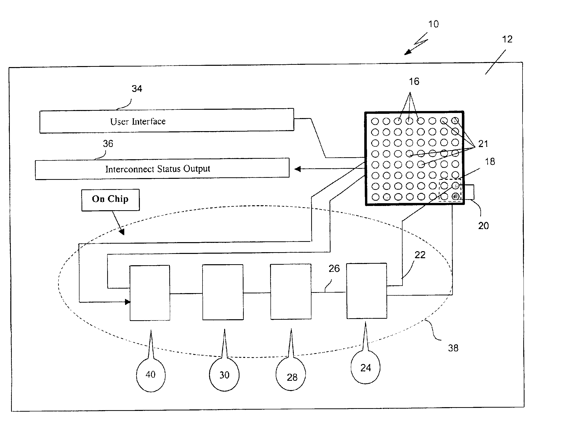
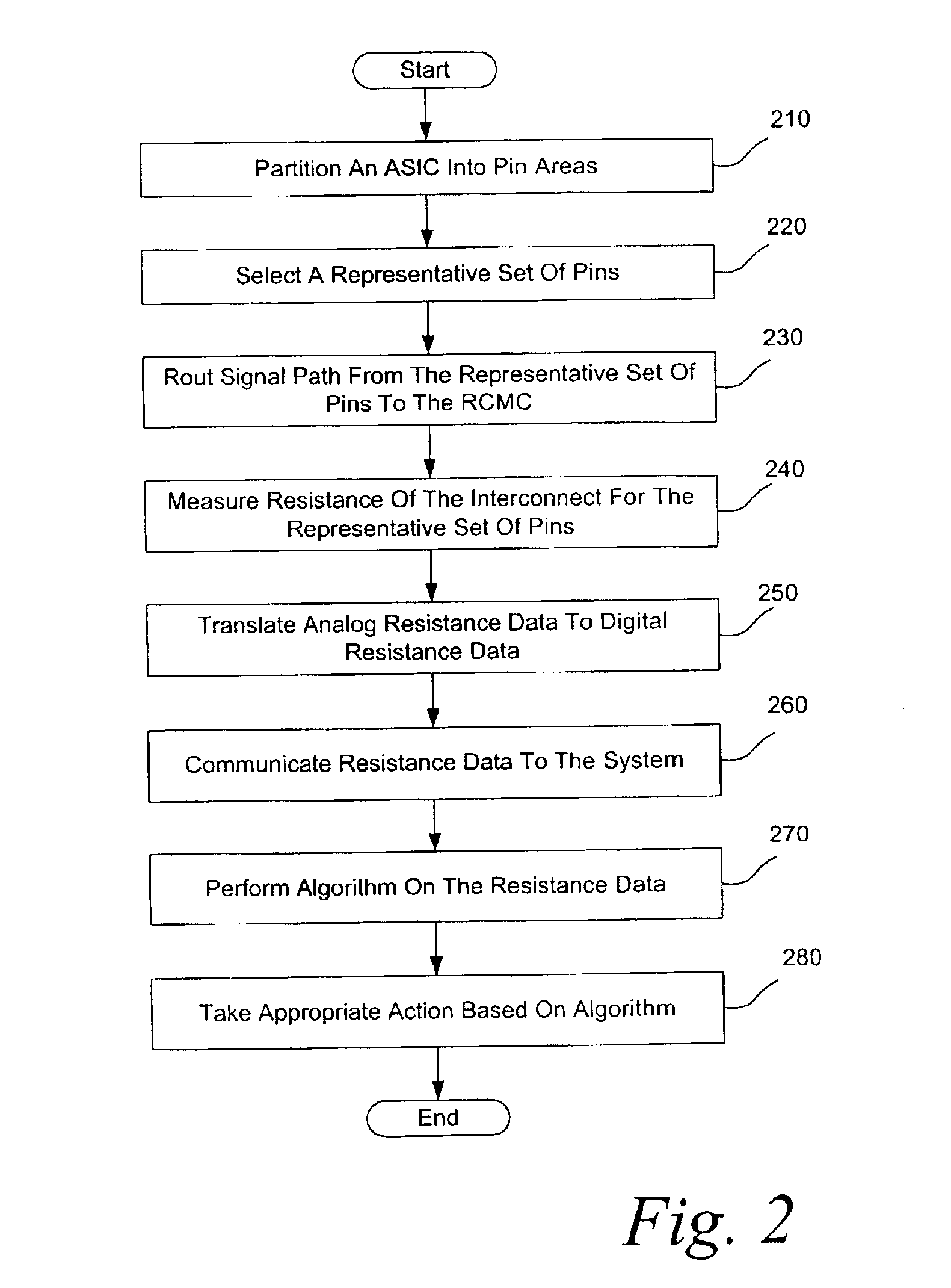
[0012]A method and corresponding apparatus for monitoring high impedance failures in chip interconnects use monitoring circuitry on a chip to provide accurate and pro-active prediction of interconnect failures. The apparatus may include a resistance continuity monitoring circuit (RCMC), and a signal path connecting a representative set of pins to the RCMC. The RCMC measures the resistance of a connection of the representative set of pins with a circuit board during system operation and outputs a measured resistance data. The apparatus further includes additional analog-to-digital (A / D) hardware to perform an analog to digital conversion of the measured resistance data. The apparatus further includes a system interface for connecting the monitoring circuitry with other system management devices. The method then performs an algorithm on the measured resistance data, potentially warning of likely interconnect failures. The algorithm may include comparing the measured resistance data wi...


PUM


Abstract

A method and corresponding apparatus for monitoring high impedance failures in chip interconnects use monitoring circuitry on a chip to provide accurate and pro-active prediction of interconnect failures. The apparatus may include a resistance continuity monitoring circuit (RCMC), and a signal path connecting a representative set of pins to the RCMC. The RCMC measures the resistance of a connection of the representative set of pins with a circuit board during system operation and outputs a measured resistance data. The apparatus further includes additional analog-to-digital (A / D) hardware to perform an analog to digital conversion of the measured resistance data. The apparatus further includes a system interface for connecting the monitoring circuitry with other system management devices. The method then performs an algorithm on the measured resistance data, potentially warning of likely interconnect failures. The algorithm may include comparing the measured resistance data with a known threshold resistance value. Alternatively, the method displays and logs the measured resistance data for further study and analysis.

Description

TECHNICAL FIELD[0001]The technical field relates to application specific integrated circuit (ASIC) design, and, in particular, to ASIC integrated method for monitoring high impedance failures in chip interconnects.BACKGROUND[0002]High impedance connections in application specific integrated circuit (ASIC) attachments can cause system failures that are extremely difficult to debug. Many new connector systems (such as sockets for ball or land grid array packages) are especially susceptible to co-planarity problems, which result in new failure modes as compared to pin and socket connectors. These failure modes present significant challenges to the design and manufacture of high quality systems. Currently there is no way to predict and proactively deal with such failure modes, since such faults don't always manifest themselves as pure ‘opens,’ which, by nature, are much easier to detect.[0003]The failure modes that result from high-impedance connections vary widely from easily detectabl...

Claims


Application Information

Patent Timeline
Patent Type & Authority Patents(United States)
IPC IPC(8): G01R31/28G06F11/00G06F11/32
CPCG01R31/2853
Inventor BARR, ANDREW H.POMARANSKI, KEN G.SHIDLA, DALE J.
Owner HEWLETT-PACKARD ENTERPRISE DEV LP
Learn More