
Magnetically actuated microelectromechanical devices and method of manufacture

a technology of magnetic actuators and microelectromechanical devices, which is applied in the field of magnetic actuator arrays of mems devices, can solve the problems of reducing the packing density of such arrays and higher insertion losses, and achieves high mirror area fill factor

Inactive Publication Date: 2005-05-17
CORNING INC
View PDF7 Cites 60 Cited by
  • Summary
  • Abstract
  • Description
  • Claims
  • Application Information

AI Technical Summary

Problems solved by technology

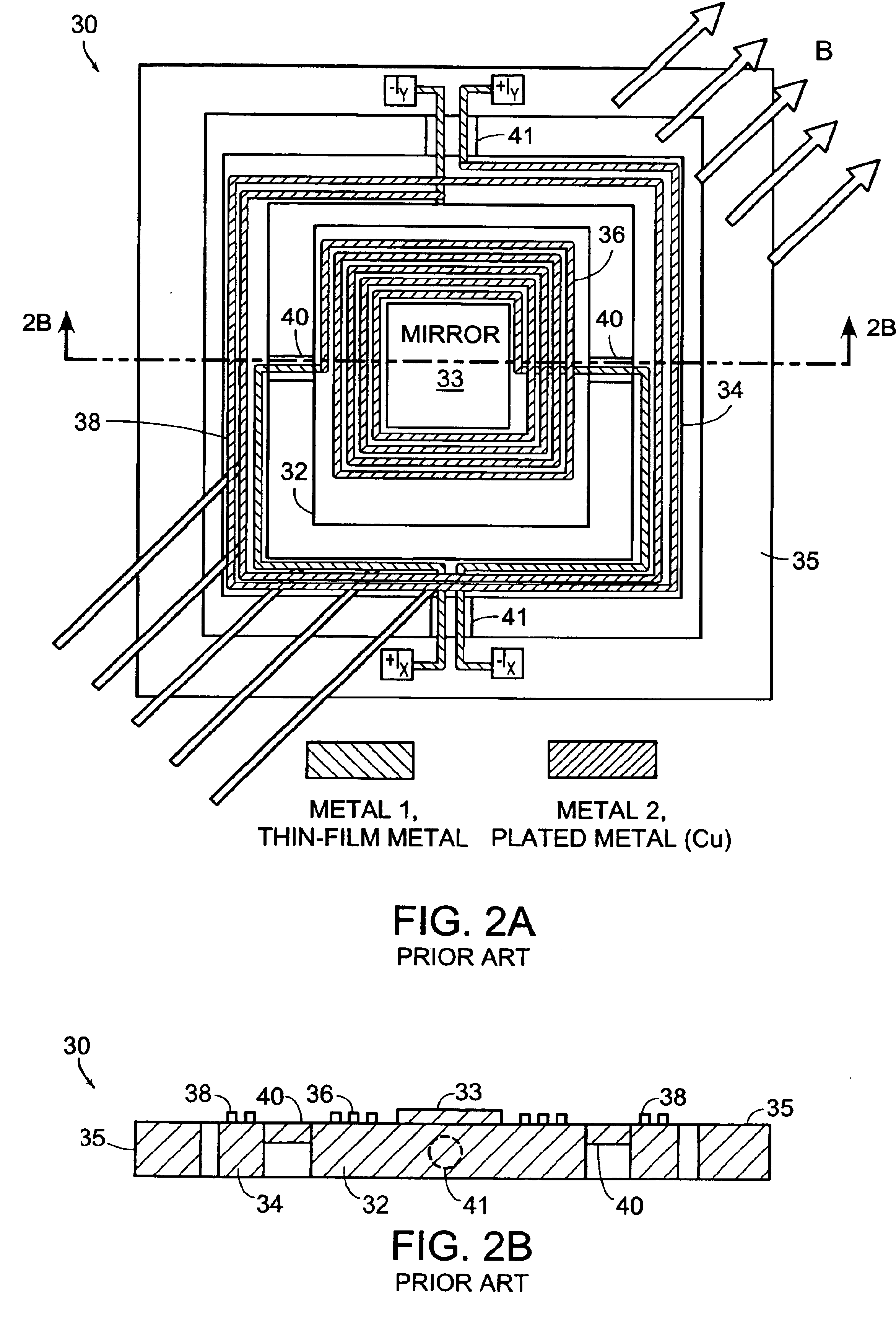
Having small mirrors is undesirable because they cannot intercept as much of an optical beam directed thereto, causing higher insertion losses.
The relatively large magnets and frame make it difficult to have multiple mirrors of this type positioned close to each other in an array thereby reducing the packing density of such arrays.

Method used


Image

  • Magnetically actuated microelectromechanical devices and method of manufacture
  • Magnetically actuated microelectromechanical devices and method of manufacture
  • Magnetically actuated microelectromechanical devices and method of manufacture

Examples


Embodiment Construction

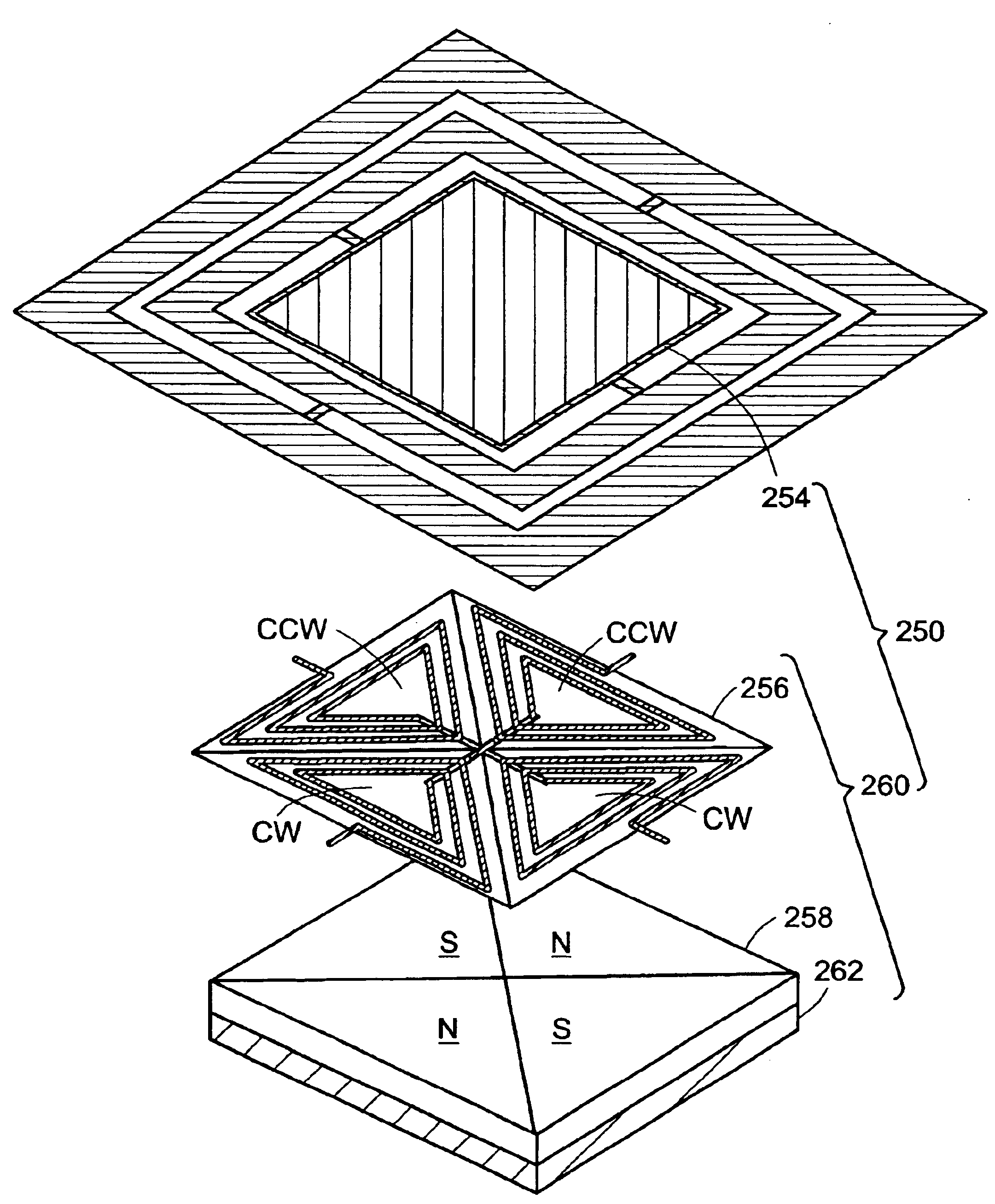
[0013]One embodiment of the invention is directed to a mirror device (for use in devices such as an optical switch, scanner or projector) having a movable mirror structure with an attached magnet. The mirror structure is movably mounted on a base structure, which includes an actuation coil for controlling movement of the mirror structure.

[0014]Another embodiment of the invention is directed to a mirror device (in a device such as an optical switch, scanner or projector) having a high mirror area fill factor. The device includes a mirror mounted on a support member, which is connected to a gimbal frame. The support member includes an enlarged portion configured to at least partially extend over the gimbal frame. The mirror substantially covers the enlarged portion of the support member, thereby providing the device with a high mirror area fill factor.

[0015]A further embodiment of the invention is directed to a mirror support structure for a movable mirror device (in a device such as ...


PUM


Abstract

One embodiment is directed to a mirror device (for a device such as an optical switch, scanner or projector) having a movable mirror structure with an attached magnet. The mirror structure is movably mounted on a base structure, which includes an actuation coil for controlling movement of the mirror structure. Another embodiment is directed to a mirror device (in a device such as an optical switch, scanner or projector) having a high mirror fill factor. The device includes a mirror mounted on a support member, which is connected to a gimbal frame. The support member includes an enlarged portion configured to at least partially extend over the gimbal frame. The mirror substantially covers the enlarged portion of the support member, thereby providing the device with a high mirror fill factor. A further embodiment is directed to a mirror support structure for a movable mirror device (in a device such as an optical switch, scanner or projector). The mirror support structure includes a post member and an enlarged lid member, one of which includes a plurality of holes and the other of which includes a corresponding plurality of projections. The post and lid members are assembled by positioning the projections in the corresponding holes.

Description

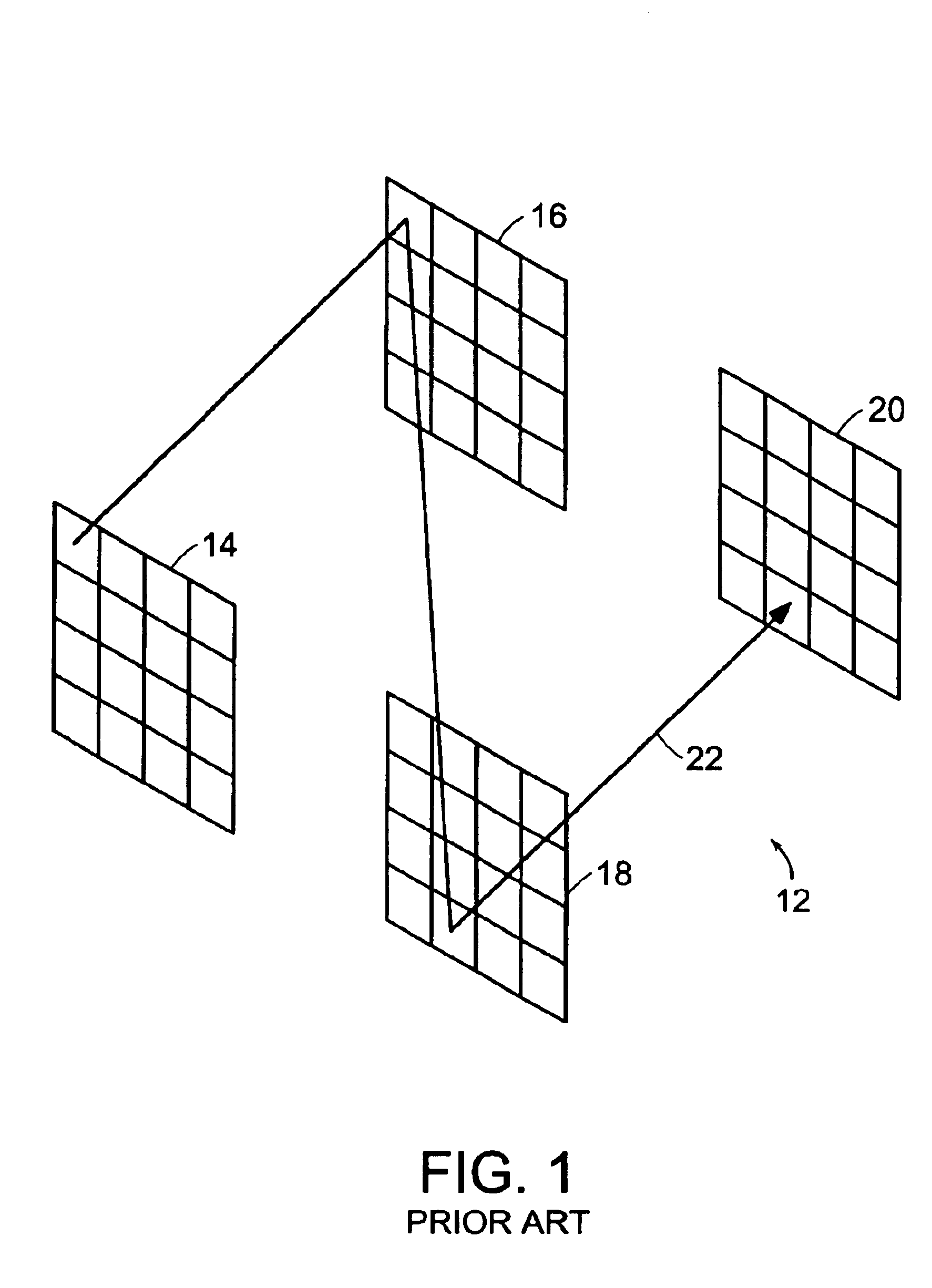
BACKGROUND OF THE INVENTION[0001]1. Field of the Invention[0002]The present invention relates generally to microelectromechanical (MEMS) devices and, in particular, to arrayed magnetically actuated MEMS devices such as arrayed mirrors used in optical switches and other devices like scanners and projectors.[0003]2. Description of Related Art[0004]FIG. 1 schematically illustrates an example of an optical cross-connect 12 of an optical switch. The cross-connect 12 includes an array of collimators or other beam-forming devices, represented by grid 14, and forms incoming optical communications signals into beams that impinge on an array of selectively moveable reflectors or mirrors represented by grid 16. Each beam from grid 14 has its own corresponding moveable mirror on grid 16.[0005]The moveable mirrors of grid 16 are controllably positioned so as to individually direct the respective beams from grid 14 to respective moveable mirrors of a second array of moveable mirrors, represented ...

Claims


Application Information

Patent Timeline
Patent Type & Authority Patents(United States)
IPC IPC(8): G02B26/08
CPCG02B26/085
Inventor TAYLOR, WILLIAM PATRICKBERNSTEIN, JONATHAN JAY
Owner CORNING INC
Learn More