Method and device for IC identification

a technology of ic and identification method, applied in the field of ic intellectual property protection, can solve the problems of time-consuming and laborious, unauthorized use of ip modules, and inability to develop ics comprising millions of logic gates or more, and achieve the effect of effective methods

Active Publication Date: 2005-04-19
NAT TAIWAN UNIV
View PDF5 Cites 6 Cited by
  • Summary
  • Abstract
  • Description
  • Claims
  • Application Information

AI Technical Summary

Benefits of technology

[0004]The goal of the present invention is to provide an effective method for detecting and verifying the use of an IP module, and solves the problems detecting the origin of an IP module used in an IC design.

Problems solved by technology

Conventional starting-from-scratch IC design approaches are unable to develop an IC comprising millions of logic gates or more in a short period of time to meet the market demands.
However, as it is technically easy to copy IP modules, and as the concept of IP protection is still in its infancy, unauthorized use of IP modules is common, and difficult to prevent.
Furthermore, when an IP module is incorporated into a chip design, it is difficult to identify the IP core from the finished layout, especially after the steps of synthesis, placement and routing.
Current technology does not provide appropriate method for detecting and verifying the use of an IP module.
This lack of IP protection may further inhibit the development of the industry.

Method used


Image

  • Method and device for IC identification
  • Method and device for IC identification
  • Method and device for IC identification

Examples


Embodiment Construction

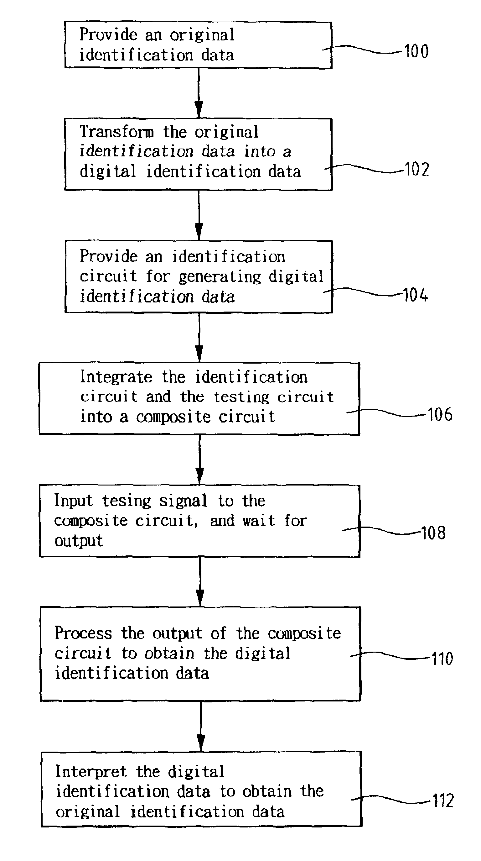
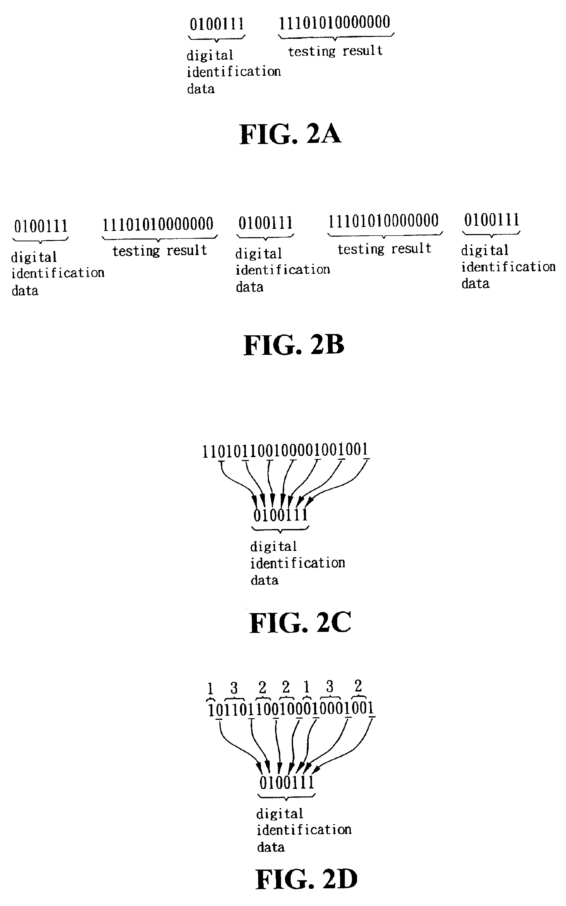
[0018]Figure a shows the flow chart of the present invention. Step 100 is to provide an original identification data to represent the origin of the IC design. The original identification data can be any of the following: the name of the original designer, the name of the designing laboratory, the name of the designing company, etc. Step 102 is to transform the original identification data into a digital identification data. A simply implementation can be as follows: if the original identification data is made of mostly alphabets, a binary string can be obtained by transforming each character of the original identification data into a 1, and each white space into a 0. The binary string is the digital identification data. Of course, other serial numbers can also be used as the digital identification data as long as they can represent the name of the designer, laboratory, or the company. Step 104 is to provide an identification circuit that can generate the digital identification data....


PUM


Abstract

The present invention provides a method for IC identification. It can be used to identify the origin of the IC design, wherein said IC comprises at least a testing circuit for testing the functional correctness of said IC, and said testing circuit is activated by a testing activation signal. The testing circuit, after receiving a testing signal, will generate a testing result. The identification method comprises the steps of (1). providing an original identification data representing the origin of the IC; (2). transforming the original identification data into a digital identification data; (3). providing an identification circuit for generating the digital identification data, wherein the identification circuit is activated by the testing activation signal, and generates the digital identification data; (4). integrating the identification circuit and the testing circuit into a composite circuit, wherein the composite circuit will be activated by the testing activation signal, receive the testing signal, process the digital identification data from identification circuit and the testing result from the testing circuit, and generate an output signal; (5). inputting the testing activation signal and the testing signal to the composite circuit, and waiting for the output signal; (6). receiving the output signal and processing the output signal to obtain digital identification data; and (7). interpreting the digital identification data to obtain the original identification data.

Description

FIELD OF THE INVENTION[0001]The invention relates to a method used in IC intellectual property protection, and more particularly to a method and a device for the detection and the verification of the origin of an IC design in order to provide legal protection in IC intellectual property.BACKGROUND OF THE INVENTION[0002]In the semiconductor industry, an integrated circuit that is designed and verified to provide certain functionality is treated as an intellectual property (IP). As the rapid development in IC design and manufacturing, more and more transistors are packed into a single chip. Conventional starting-from-scratch IC design approaches are unable to develop an IC comprising millions of logic gates or more in a short period of time to meet the market demands. Instead, by integrating one or more IP modules into a single chip, the IC developers can design chips that provide multiple functions a complete system, called system on a chip (SOC). For example, a chip used in computer...

Claims


Application Information

Patent Timeline
IPC IPC(8): G06F17/50G01R31/317
CPCG01R31/31707G01R31/31719G01R31/31718
Inventor TSAO, HEN-WAIFAN, YU-CHENG
Owner NAT TAIWAN UNIV
Why Eureka
Try Eureka