
Method of manufacturing semiconductor device

a manufacturing method and semiconductor technology, applied in the field of semiconductor devices, can solve the problems of significant problem of ingaas-base hbts, difficult to apply ingaas-base hbts as semiconductor devices for power amplifiers for use in mobile communication tools, and difficult to manufacture hbts on a six-inch gaas substrate, etc., and achieve low cost and good high-frequency characteristics.

Inactive Publication Date: 2005-04-19
HITACHI LTD
View PDF4 Cites 8 Cited by
  • Summary
  • Abstract
  • Description
  • Claims
  • Application Information

AI Technical Summary

Benefits of technology

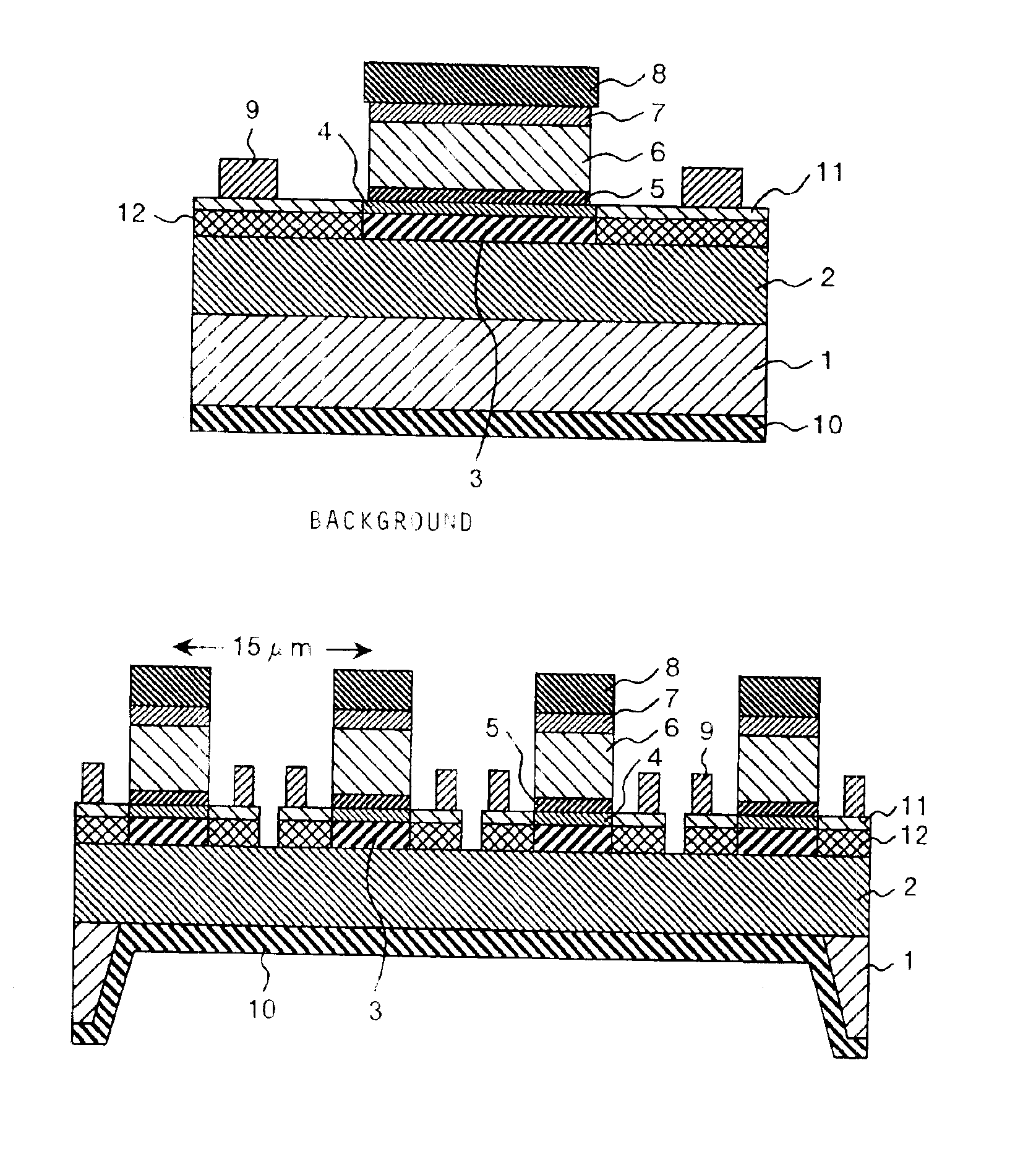
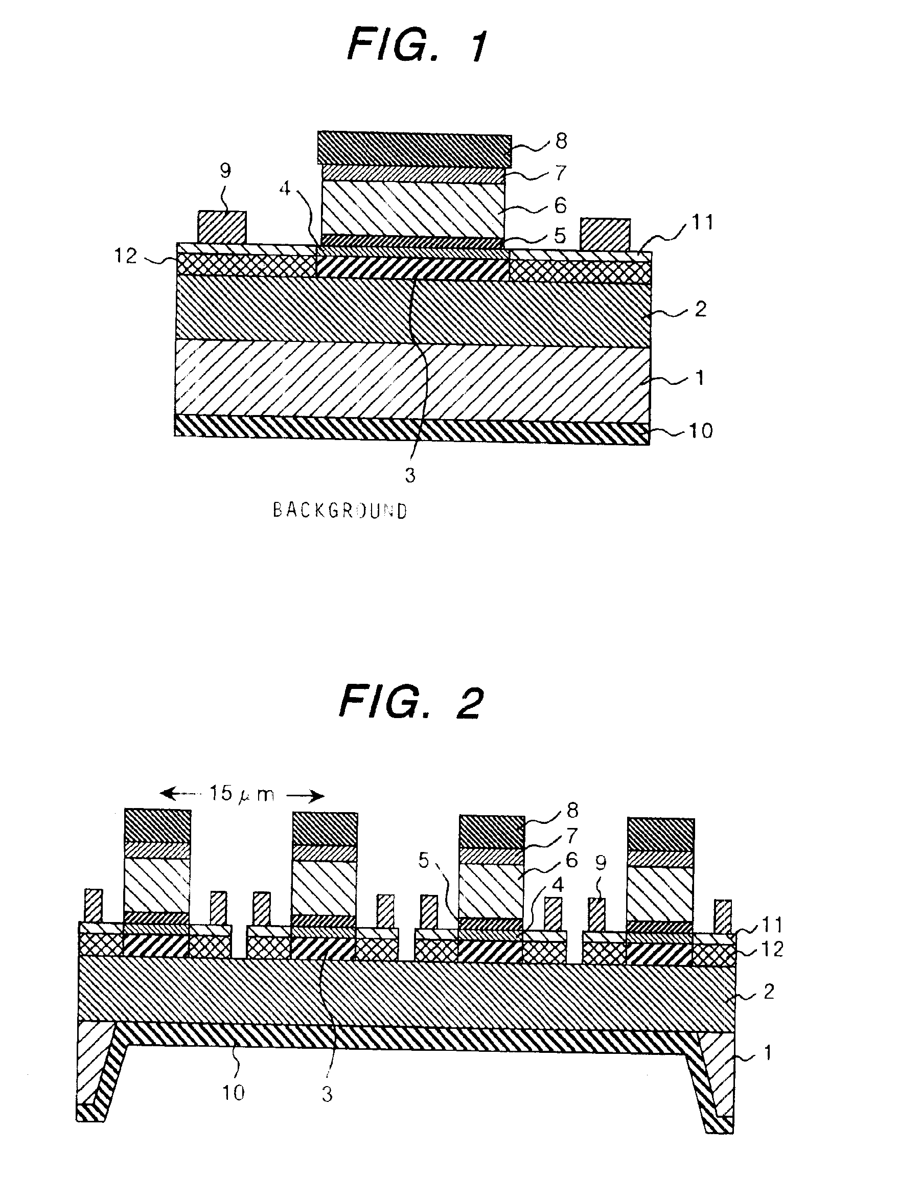
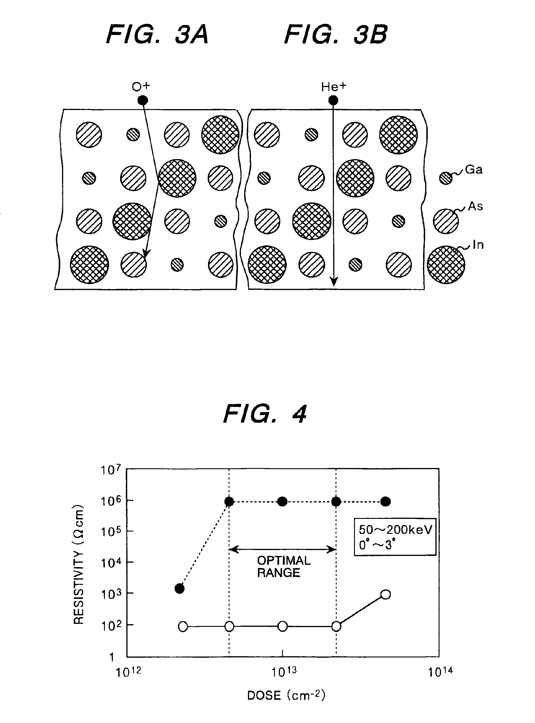
The present invention provides a method for manufacturing semiconductor devices using InGaAs-based HBTs at a low cost without compromising their high-frequency characteristics. This is achieved by implanting helium ions into an external base layer in a specific way. This method results in highly resistive n-type InAlAs external emitter regions while maintaining the p-type conductivity of the p-type InGaAs external base regions.

Problems solved by technology

Although the InGaAs-base HBTs have excellent high-frequency characteristics, the size of the InP substrate which lattice matches with InGaAs (the mole fraction of InAs is 0.5) is restricted to a maximum of four inches, and, therefore, the unit cost of these transistors is about three times as high as HBTs fabricated on a six-inch GaAs substrate.
Because of the cost consideration, it has been difficult to apply the InGaAs-base HBTs as semiconductor devices for power amplifiers for use in mobile communication tools for which low price is required.
However, a significant problem of InGaAs-base HBTs was posed in relation to ion implantation which is an essential process for fabricating C-top HBTs.
This phenomenon makes the ohmic contact of the base electrode inoperative and, consequently, made the transistor impossible to operate as a C-top HBT.
However, this method of re-implantation of p-type impurities such as Be into the base layer cannot be applied for the following reason.
In addition to higher cost by the increased number of processes, annealing at 800° C. or higher is required to activate the impurities and this has an adverse effect on the characteristics of the transistor with the InGaAs base layer because InGaAs changes its properties when exposed to temperature of 500° C. or higher.
Therefore, it has heretofore been difficult to manufacture InGaAs-base C-top HBTs having good high-frequency characteristics at low cost.

Method used


Image

  • Method of manufacturing semiconductor device
  • Method of manufacturing semiconductor device
  • Method of manufacturing semiconductor device

Examples


embodiment

[0053]FIG. 8 is a schematic cross section diagram of a power amplifier module for mobile equipment, the module fabricated, using the MMIC including the InGaAs-base C-top HBTs, described in Embodiment 2. For this module package, a glass ceramic substrate with a relative dielectric constant of 8 is employed, which was produced by low temperature firing. Owing to the reduced MMIC size which is one fourth the size of conventional MMICs, the module size is 4 mm by 4 mm, which is significantly smaller than the corresponding module size of 6 mm by 6 mm achieved by prior art. Reference numeral 101 denotes a metal cap, 102 denotes a chip part including external capacitors, inductors, and resistors. Reference numeral 103 denotes an electric line which is formed by thick film screen print of Ag and PT laminated films. Reference numeral 105 denotes the MMIC of Embodiment 2 and its bottom surface is electrically bonded to a ground layer 108 by Ag paste. The leads of the input electrode pad PIN a...


PUM


Abstract

The present invention provides a method of manufacturing semiconductor devices, by which InGaAs-base C-top HBTs are manufactured at low cost. Helium ions with a smaller radius are implanted into a p-type InGaAs layer (in external base regions) not covered with a lamination consisting of an undoped InGaAs spacer layer, n-type InP collector layer, n-type InGaAs cap layer, and collector electrode from a direction vertical to the surface of the external base layer or within an angle of 3 degrees off the vertical. In consequence, the p-type InGaAs in the external base regions remains p-type conductive and low resistive and the n-type InAlAs layer in the external emitter regions can be made highly resistive. By this method, InGaAs-base C-top HBTs can be fabricated on a smaller chip at low cost without increase of the number of processes.

Description

BACKGROUND OF THE INVENTION[0001]1. Field of the Invention[0002]The present invention relates to semiconductor devices using Collector-top Heterojunction Bipolar Transistors (hereinafter referred to as C-top HBTs) in which an InGaAs base layer is employed and a collector layer is formed on the top of the surface of the InGaAs base layer. In particular, the invention relates to a method of manufacturing semiconductor devices which are ideal for power amplifiers for use in mobile communication tools for which high electric power conversion efficiency is required.[0003]2. Description of the Related Art[0004]Along with rapid growth of mobile communication equipment, study and development of power amplifiers for use in such communication equipment have lately been conducted actively. In order to enhance the electric power conversion efficiency of a power amplifier, it is necessary to enhance the electric power conversion efficiency of the HBTs employed in the power amplifier. For this pu...

Claims


Application Information

Patent Timeline
Patent Type & Authority Patents(United States)
IPC IPC(8): H01L21/331H01L21/70H01L29/66H01L21/02H01L21/8252H01L29/737H01L27/06H03F3/189H03F3/19H03F1/30H01L21/265H01L21/8222
CPCH01L21/263H01L21/8252H01L27/0605H03F3/19H01L29/7371H03F1/302H01L29/66318H01L29/20H01L21/18
Inventor MOCHIZUKI, KAZUHIROOUCHI, KIYOSHITANOUE, TOMONORI
Owner HITACHI LTD
Learn More