Image forming system and image forming method for deciding AC voltage to be applied to charger
a technology of image forming system and charger, which is applied in the direction of electrographic process apparatus, instruments, corona discharge, etc., can solve the problems of image escape, image degradation, wear acceleration, etc., and achieve the effect of high image quality over a long tim
- Summary
- Abstract
- Description
- Claims
- Application Information
AI Technical Summary
Benefits of technology
Problems solved by technology
Method used
Image
Examples
first embodiment
A first embodiment of the invention is explained with reference to FIGS. 1-8.
(System Structure)
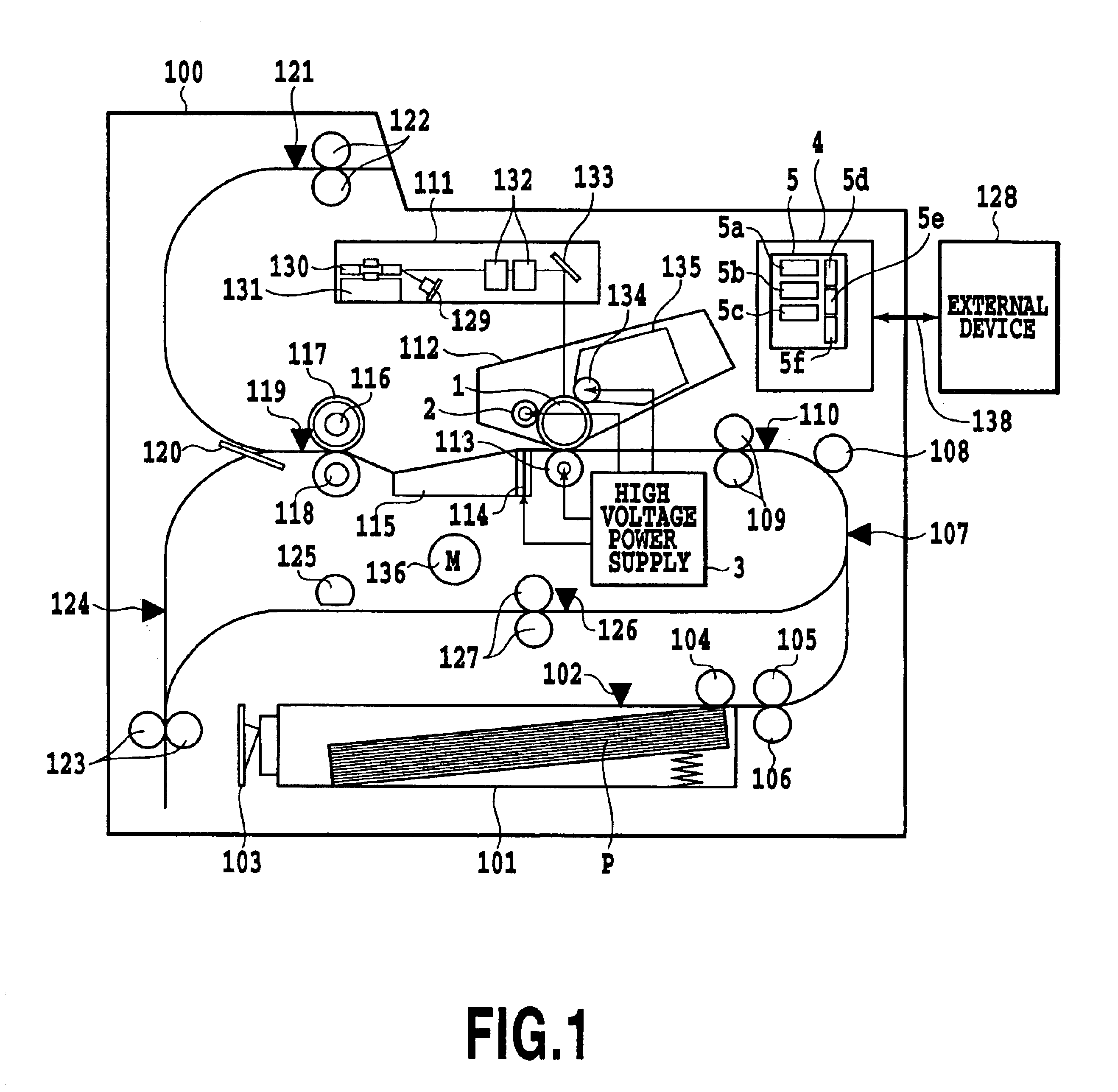
FIG. 1 is an example of the structure of a laser printer 100 that belongs to the image forming system of the present invention.
The laser printer 100 has a deck 101 holding recording paper P. The deck 101 has a deck sensor 102 that detects the presence / absence of recording paper p, a paper size sensor 103 that detects the size of recording paper p, and a pickup roller 104 that picks up recording paper P. The laser printer 100 further comprises a deck paper transport roller 105 that transports recording paper P picked up by the pickup roller 104 and a retard roller 106 that works with the deck paper transport roller 105 to prevent recording paper P from being stacked during transport.
In the downstream of the deck paper transport roller 105 installed are a feeder sensor 107 that detects the state of paper sent from the deck 101 and a turn-over unit for double-sided printing(to be described la...
second embodiment
Now a second embodiment of the invention will be explained with reference to FIGS. 9-11. The same components as those of the first embodiment have the same numbers and their descriptions are not repeated here.
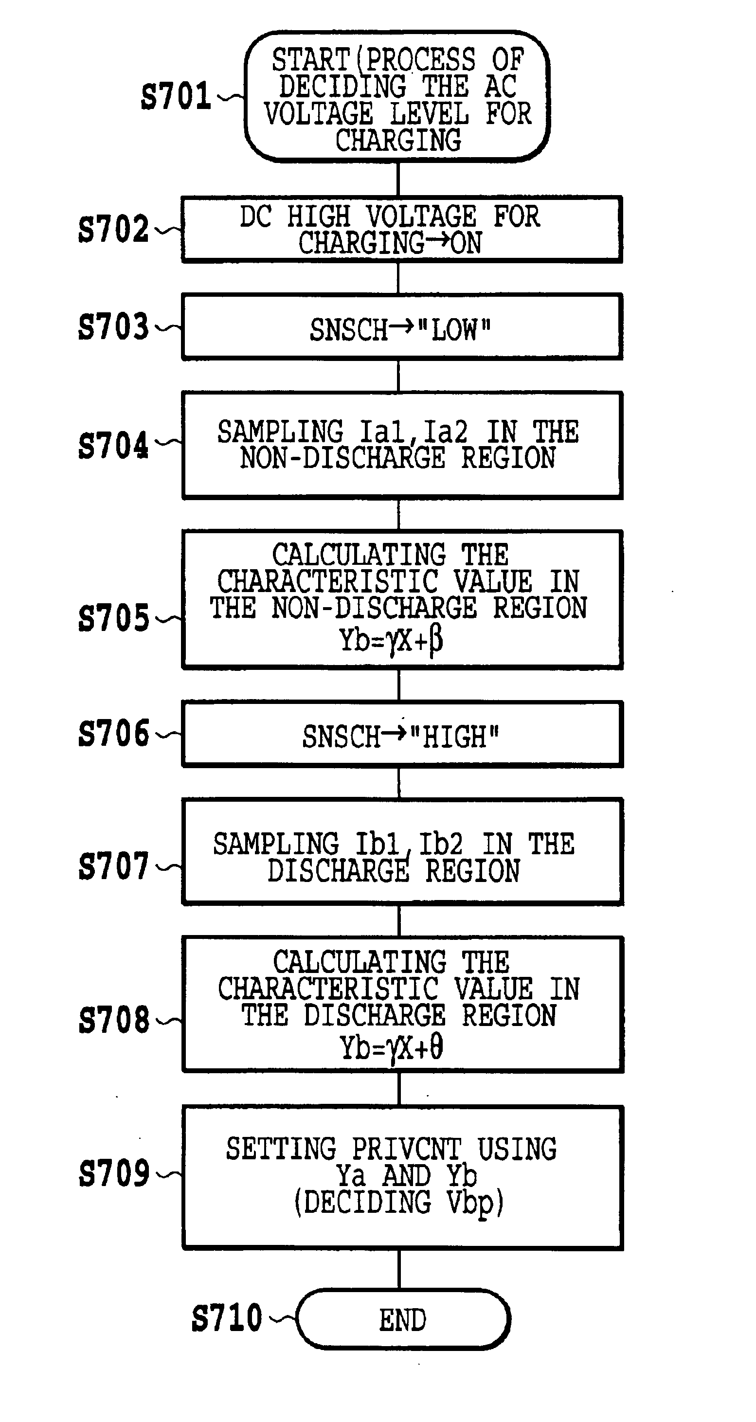
In the above first embodiment, the detection characteristics of detection current have been switched between the non-discharge region and the discharge region when the AC charge current, which is produced by AC high voltage for charging, is measured.
The charging output control circuit of the image forming system of this embodiment has two charge current detection units of different current detection characteristics, and these current detection units are selectively switched between the non-discharge region and the discharge region.
(Structure of the Charging Output Control Circuit)
FIG. 9 shows an example of the charge output control circuit of the invention.
The charge output control circuit is roughly divided into a first AC charge current detection unit, a second AC charge curr...
PUM
 Abstract
Description
Claims
Application Information
 - R&D
- Intellectual Property
- Life Sciences
- Materials
- Tech Scout
- Unparalleled Data Quality
- Higher Quality Content
- 60% Fewer Hallucinations
Browse by: Latest US Patents, China's latest patents, Technical Efficacy Thesaurus, Application Domain, Technology Topic, Popular Technical Reports.
© 2025 PatSnap. All rights reserved.Legal|Privacy policy|Modern Slavery Act Transparency Statement|Sitemap|About US| Contact US: help@patsnap.com


