Rapidly testable semiconductor memory device

a memory device and semiconductor technology, applied in the direction of information storage, static storage, digital storage, etc., can solve the problems of inability to know which of the two memory cells being compared is defective, the type of test takes considerable time, and the problem becomes irrelevan

Inactive Publication Date: 2005-03-15
LAPIS SEMICON CO LTD
View PDF5 Cites 23 Cited by
  • Summary
  • Abstract
  • Description
  • Claims
  • Application Information

AI Technical Summary

Benefits of technology

A general object of the present invention is to speed up the testing of a semiconductor memory device.
Another general object of the invention is to increase the number of defects that can be repaired in a semiconductor memory device.
Another more specific object is to provide a semiconductor memory device that can be repaired by replacing only memory cells in a single memory cell array that are read by a single sense amplifier array.
Tertiary decision circuits may be provided to compare the results obtained by the secondary decision circuits. The tertiary decision circuits can be advantageously used to output screening test results through a reduced number of external input-output terminals.

Problems solved by technology

Defects can be found by writing known data into all memory cells, then reading the data, but this type of test takes considerable time.
A problem with this scheme is that when a defective bit is detected, it is not known which of the two memory cells being compared is defective.
If the memory device has redundant columns and each redundant column spans all the memory cell arrays, a conventional arrangement that has often been used in the past, the above problem becomes irrelevant, since both of the compared memory cells are replaced.
This conventional arrangement unduly limits the number of defects that can be repaired, however.
If a defect in a particular column is limited to a particular memory cell array, it is obviously inefficient to replace the same column in other, non-defective memory cell arrays.

Method used


Image

  • Rapidly testable semiconductor memory device
  • Rapidly testable semiconductor memory device
  • Rapidly testable semiconductor memory device

Examples


first embodiment

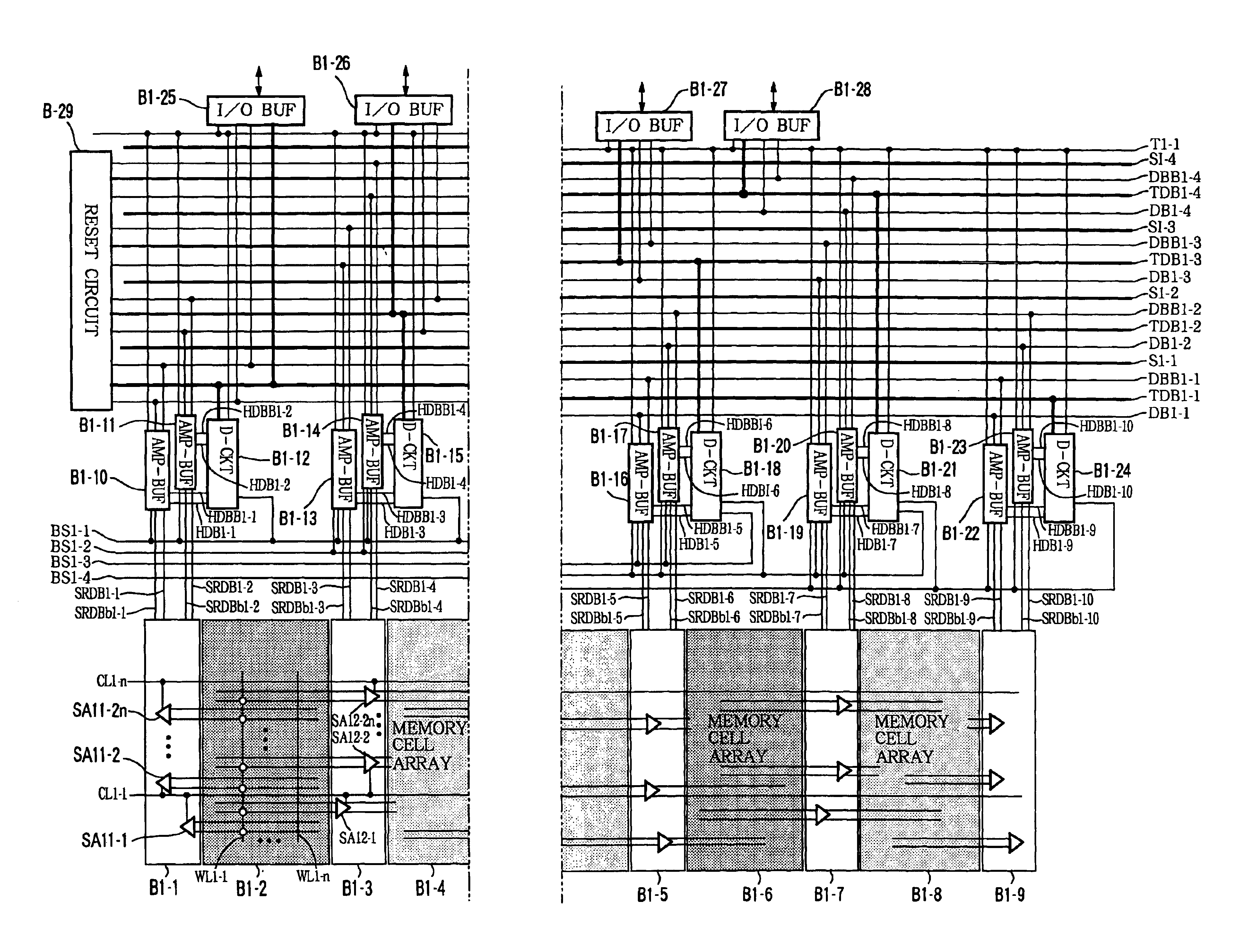
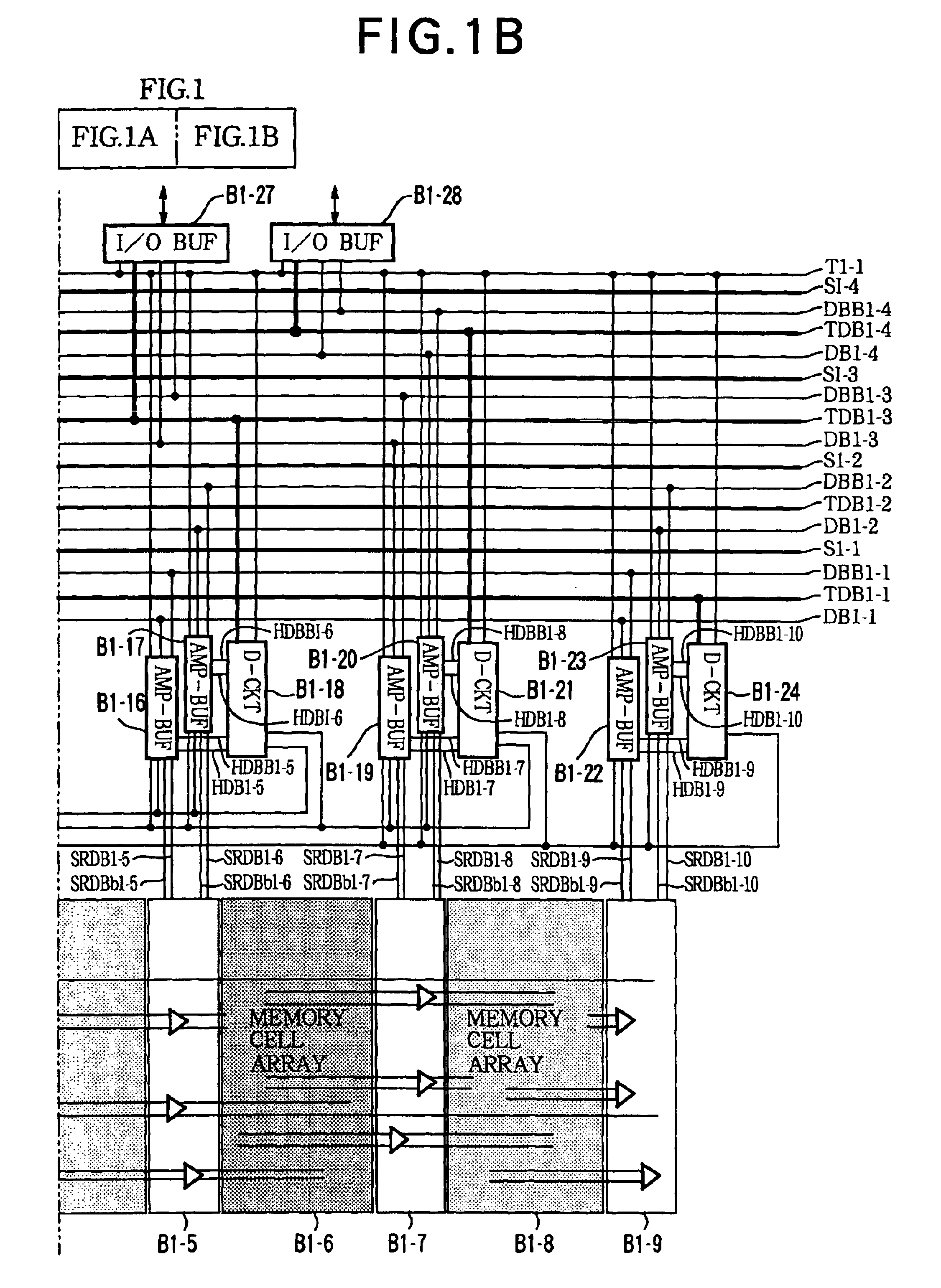
Referring to FIGS. 1A and 1B, the first embodiment of the invention is a semiconductor memory device comprising four memory cell arrays B1-2, B1-4, B1-6, B1-8 interspersed among five sense amplifier arrays B1-1, B1-3, B1-5, B1-7, B1-9. The memory cell arrays are spanned by n column lines CL1-1 to CL1-n, where n is an integer greater than one. Each column line activates four sense amplifiers adjacent each memory cell array: for example, the first column line CL1-1 activates sense amplifiers SA11-1 and SA11-2 in the sense amplifier array B1-1 on one side of memory cell array B1-2 and sense amplifiers SA12-1 and SA12-2 in the sense amplifier array B1-3 on the other side of memory cell array B1-2. Each sense amplifier is coupled to a complementary pair of bit lines extending across the adjacent memory cell array or arrays. Each memory cell array includes n word lines WL1-1 to WL1-n, and n×n memory cells, indicated by white circles, disposed at alternate intersections of the word lines a...

second embodiment

The second embodiment enables a semiconductor memory device with twice the memory capacity of the device in the first embodiment to be tested in the same space of time as in the first embodiment. The number of defective columns that can be repaired in each memory cell array is less than in the first embodiment, however, because the scheme illustrated in FIGS. 8A and 8B cannot be used.

Third Embodiment

Referring to FIGS. 16A, 16B, and 16C, the third embodiment comprises the same sense amplifier arrays, memory cell arrays, output amplifier-input buffers, primary and secondary decision circuits, input-output buffers, reset circuit, data bus lines, read data bus lines, comparison data bus lines, test data bus lines, shield lines, and block select signal lines as the second embodiment. These elements are indicated by the same reference characters as in the second embodiment, except that ‘B3’ and ‘S3’ are changed to ‘B4’ and ‘S4’: for example, the first sense amplifier array is now designat...

third embodiment

The third embodiment thus provides the combined effects of the first and second embodiments.


PUM


Abstract

A semiconductor memory device has an array of memory cells, an array of sense amplifiers selected at least two at a time by column lines, data bus lines that receive data read from the memory cell array by the selected sense amplifiers, a decision circuit that compares data read by two of the selected sense amplifiers, and an input-output buffer. Normally, the input-output buffer receives and outputs data from one or more of the data bus lines. In a test output mode, the input-output buffer receives and outputs comparison result data from the decision circuit. In a semiconductor memory device with multiple memory cell arrays, this arrangement enables data read from different memory cells in the same memory cell array to be compared, so that redundancy repair can be carried out efficiently.

Description

BACKGROUND OF THE INVENTION1. Field of the InventionThe present invention relates to redundancy repair of a semiconductor memory device. More particularly, it relates to the rapid identification and efficient repair of defective memory cells.2. Description of the Related ArtLarge-scale integrated semiconductor memory devices generally have redundant rows or columns of memory cells that can be used to replace defective rows or columns if the defect is found before the device is packaged. Defects can be found by writing known data into all memory cells, then reading the data, but this type of test takes considerable time. A faster way to test the memory device is to write known data into all memory cells, then compare the data in pairs of memory cells and read the comparison results, thereby reducing the read-out time by half.A conventional semiconductor memory device employing this type of comparison test includes a plurality of memory cell arrays. After identical data have been writ...

Claims


Application Information

Patent Timeline
Patent Type & Authority Patents(United States)
IPC IPC(8): G11C29/44G11C29/00G11C29/04
CPCG11C29/1201G11C29/846G11C29/781G11C29/44
Inventor TANABE, TETSUYANASU, NOBUTAKA
Owner LAPIS SEMICON CO LTD
Why Eureka
Try Eureka