Apparatus for reading marks on a semiconductor substrate

Inactive Publication Date: 2005-03-15
ADVANCED MICRO DEVICES INC
View PDF10 Cites 0 Cited by
  • Summary
  • Abstract
  • Description
  • Claims
  • Application Information

AI Technical Summary

Benefits of technology

The present invention satisfies the foregoing need by providing an apparatus and a method for reading marks on objects such as, for example, a semiconductor wafer. In a preferred embodiment of an apparatus for reading marks incorporating features of the present invention, a wafer receptacle having a slot formed therein is coated on at least one side with a mirror material. The wafer receptacle is spaced apart from a base plate in a beveled or angled fashion. A back support is coupled between the wafer receptacle and the base plate. Optionally, a concave mirror may be coupled to the base plate. When the concave mirror is coupled to the base plate, the back support serves as a wafer reading side. Moreover, light sources may be coupled to the apparatus to increase the amount of light available to carry the images.

Problems solved by technology

These scribe readers have a large number of moving parts, use very sophisticated circuitry, and are expensive to maintain and operate.

Method used


Image

  • Apparatus for reading marks on a semiconductor substrate
  • Apparatus for reading marks on a semiconductor substrate
  • Apparatus for reading marks on a semiconductor substrate

Examples


Embodiment Construction

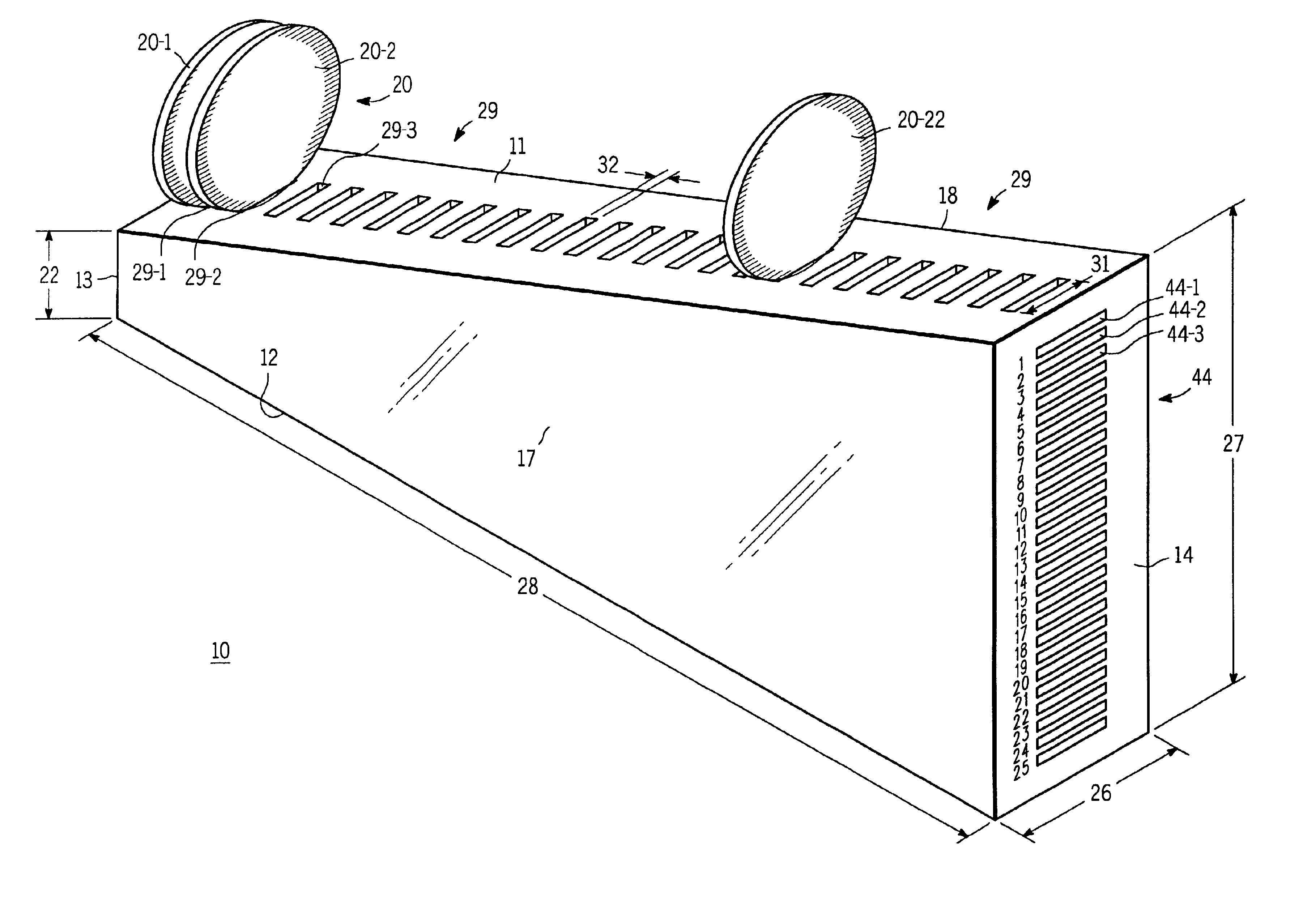
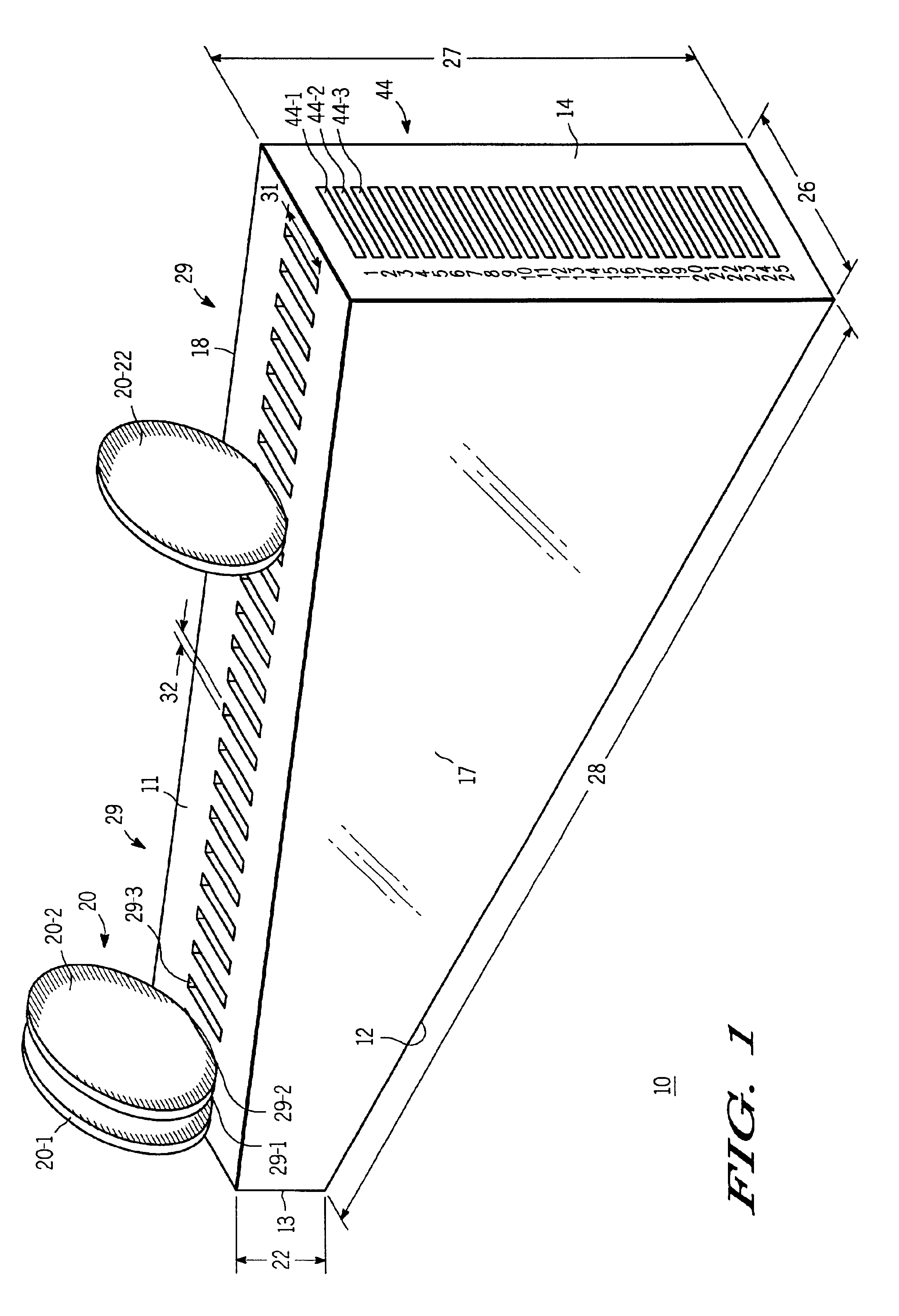
FIG. 1 is an isometric view of an apparatus 10 for reading marks on an object in accordance with an embodiment of the present invention. When used for reading scribe marks on a semiconductor wafer, apparatus 10 is referred to as a scribe reader. In accordance with a first embodiment, scribe reader 10 comprises a wafer receptacle or top plate 11 spaced apart from a bottom or base plate 12, a front support 13 spaced apart from and substantially parallel to a back support 14, and a vertical support 17 spaced apart from and substantially parallel to an opposing vertical support 18. Wafer receptacle 11 is also referred to as a wafer support side, and back support 14 is also referred to as a scribe mark reader side, a mark reading side, or a wafer reading area. By way of example, wafer receptacle 11, base plate 12, front support 13, and back support 14 are each rectangularly shaped sections that are coupled together to form the body of scribe reader 10. Wafer receptacle 11 and base plate ...


PUM


Abstract

An apparatus and a method for reading a mark on a wafer. The apparatus includes a wafer receptacle having a mirror material coated on one side and a plurality of slots formed therein. The wafer receptacle is coupled to a base plate via a back support. The apparatus may also include a front support coupled between the wafer receptacle and the base plate. A plurality of concave mirrors are coupled to the base plate. A wafer placed in one of the plurality of slots reflects light to the mirror material coating the wafer receptacle. The light is reflected by the mirror material to one of the concave mirrors, which rectifies an image contained in the light and reflects the rectified image to the back support. The image can be viewed on the back support.

Description

FIELD OF THE INVENTIONThis invention relates, in general, to semiconductor manufacturing and, more particularly, to apparatuses and methods for reading marks on semiconductor substrates.BACKGROUND OF THE INVENTIONIntegrated circuits and discrete semiconductor devices are typically fabricated on wafers made from semiconductor substrates such as, for example, silicon, silicon germanium, gallium arsenide, indium phosphide, and the like. The semiconductor wafers have either a positioning notch or a flat edge for aligning the wafers and scribe marks for individual wafer identification. Scribe marks are small alphanumeric sequences formed on the wafer by chemical etching, laser cutting, or other techniques capable of making a well defined mark on a semiconductor wafer. These marks are located close to the positioning notch or the flat edge of the semiconductor wafer. Because scribe marks are used for identifying individual semiconductor wafers, it is very important for semiconductor devic...

Claims


Application Information

Patent Timeline
IPC IPC(8): G01N21/01H01L21/00H01L21/673
CPCH01L21/67313H01L21/67294
Inventor KLINGEMANN, RAYMOND E.MCCARTHY, MICHAEL
Owner ADVANCED MICRO DEVICES INC
Why Eureka
Try Eureka