
Buffer metal layer

a buffer metal and layer technology, applied in the direction of semiconductor devices, semiconductor/solid-state device details, electrical devices, etc., can solve the problems of inability to properly function of integrated circuits, inability to meet the requirements of manufacturing, and every solution tends to produce new problems, etc., to achieve high thermal conductivity, high structural strength, and the effect of dissipation of hot spots

Inactive Publication Date: 2005-03-01
BELL SEMICON LLC
View PDF6 Cites 0 Cited by
  • Summary
  • Abstract
  • Description
  • Claims
  • Application Information

AI Technical Summary

Benefits of technology

The above and other needs are met by an integrated circuit having a top passivation layer and bonding pads, where the improvement is a metal layer overlying substantially all of the integrated circuit. The metal layer overlies the top passivation layer and is not in electrical contact with any of the bonding pads. In this manner, there is a structure that is added to the integrated circuit which has a relatively high thermal conductivity, and which also has a, relatively high structural strength. With these two added properties, the occurrence of stress cracks, such as those induced by plastic molded packages, is reduced, and hot spots tend to be dissipated. Thus, the overlying metal layer tends to improve the reliability of the integrated circuit.
According to another aspect of the invention, there is described an integrated circuit having a top passivation layer and bonding pads, where the improvement is a metal layer overlying substantially all of the integrated circuit. The metal layer overlies the top passivation layer and is only in electrical contact with ground contacts of the bonding pads. In this manner, there is a structure that is added to the integrated circuit which has a relatively high thermal conductivity, and which also has a relatively high structural strength, the benefits of which are described above. However, with the metal layer grounded to one or more of the bonding pads, the metal layer also provides electromagnetic radiation shielding. Although the metal layer can provide some degree of electromagnetic radiation shielding even when it is not grounded to a bonding pad, grounding the metal layer in this manner tends to enhance the electromagnetic radiation shielding.

Problems solved by technology

Because integrated circuits tend to be extremely sensitive devices, there are a great many constraints that are placed on their designs.
Often, these constraints are interrelated, and may even be conflicting in nature.
It an integrated circuit cracks, then the various layers tend to not make proper electrical and physical connections one with the other, and the integrated circuit does not function properly.
Unfortunately, every solution tends to produce new issues.
In the case of plastic molding, localized formations of thermal energy, or hot spots, tend to occur because the plastic molding is not a good heat conductor.
Also, because the plastic molding tends to have a different thermal coefficient of expansion than the other elements of the integrated circuit, there is a tendency for plastic molded integrated circuits to develop stress cracks, such as at the corners of such devices.
As another example, even without the thermal insulating effects of a molded plastic package, integrated circuits tends to develop hot spots in certain locations.
Silicon and other semiconducting materials are relatively poor thermal energy conductors, and thus when a specific portion of an integrated circuit has a relatively heavy duty cycle, the thermal energy that is developed by the electrical activity in that area tends to build up in that area, rather than to dissipate to other areas.

Method used


Image

  • Buffer metal layer
  • Buffer metal layer

Examples


Embodiment Construction

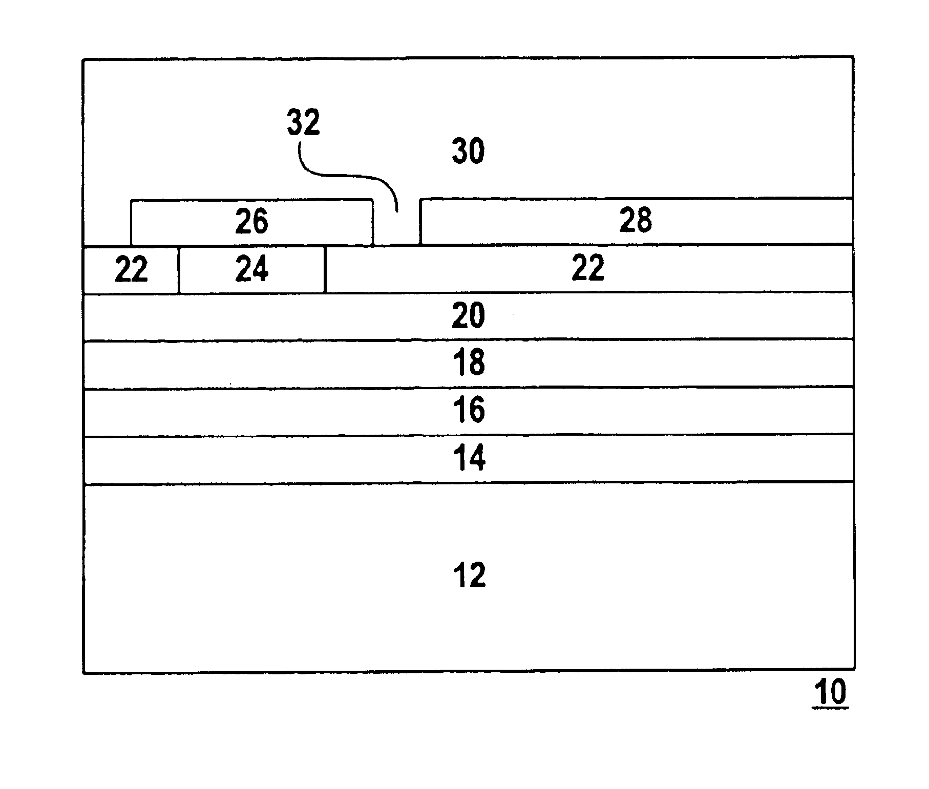
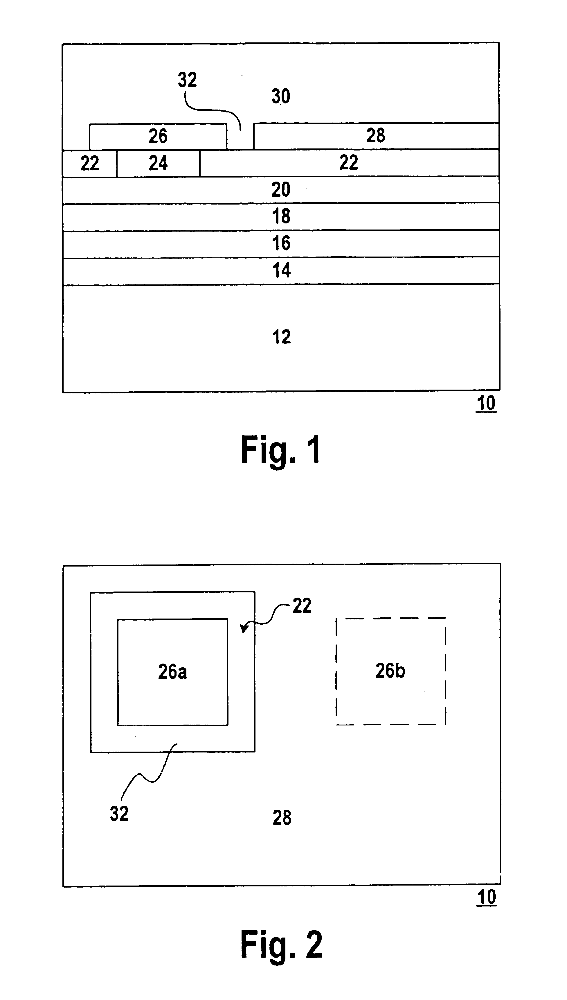
With reference now to FIG. 1 there is depicted a cross sectional view of an integrated circuit 10, depicting the relationship between the passivation layer 22, the metal layer 28, the bonding pads 26, and the packaging 30. As depicted in FIG. 1, the integrated circuit 10 is fabricated on a substrate 12, which is most preferably a semiconducting substrate such as germanium, silicon germanium, a III-IV material such as gallium arsenide, or most preferably silicon. Layers 14-16 are built up on the substrate 12 in a manner as known in the art, to form the various structures, elements, and components, both active and passive, of the integrated circuit 10. It is appreciated that in actual implementation, there would tend to be a far greater number of such layers 14-16, and the structures so formed would not all be planar as depicted in FIG. 1. Therefore, the layers 14-16 are representational only, and are not intended to be a limitation on the present invention in any way.

Layer 20 represe...


PUM


Abstract

An integrated circuit having a top passivation layer and bonding pads, where the improvement is a metal layer overlying all of the integrated circuit. The metal layer overlies the top passivation layer and is not in electrical contact with any of the bonding pads. In this manner, there is a structure that is added to the integrated circuit which has a relatively high thermal conductivity, and which also has a relatively high structural strength. With these two added properties, the occurrence of stress cracks, such as those induced by plastic molded packages, is reduced, and hot spots tend to be dissipated. Thus, the overlying metal layer tends to improve the reliability of the integrated circuit.

Description

FIELDThis invention relates to the field of integrated circuit fabrication. More particularly, this invention relates to improving the structural, heat dissipation, and electrical shielding properties of an integrated circuit.BACKGROUNDBecause integrated circuits tend to be extremely sensitive devices, there are a great many constraints that are placed on their designs. These constraints typically fall into one or more general categories such as structural constraints, issues dealing with heat dissipation, and electrical shielding of the integrated circuit. Often, these constraints are interrelated, and may even be conflicting in nature.For example, in regard to structural constraints, an integrated circuit needs to be protected in a manner where it will not crack. It an integrated circuit cracks, then the various layers tend to not make proper electrical and physical connections one with the other, and the integrated circuit does not function properly. Thus, various methods have be...

Claims


Application Information

Patent Timeline
IPC IPC(8): H01L23/52H01L23/522H01L23/367H01L23/34H01L23/373H01L23/552
CPCH01L23/367H01L23/5222H01L23/552H01L23/3735H01L2924/0002H01L2924/00
Inventor CHIA, CHOK J.LOW, QWAI H.RANGANATHAN, RAMASWAMY
Owner BELL SEMICON LLC
Learn More