
Substrate processing apparatus and related systems and methods

Inactive Publication Date: 2005-01-25
BOC EDWARDS
View PDF73 Cites 118 Cited by
  • Summary
  • Abstract
  • Description
  • Claims
  • Application Information

AI Technical Summary

Benefits of technology

[0009]The design of the apparatus allows the inner volume of the second chamber to contain and maintain a controlled atmosphere of an appropriate gas (e.g., nitrogen) at substantially ambient pressure when the second chamber is either open or closed and the first chamber is either open or closed. The design of the apparatus further allows the inner volume of the second chamber to contain and maintain a controlled atmosphere of gas at substantially ambient pressure or sub-atmospheric pressure when the second chamber is closed and the first chamber is either open or closed. Moreover, the design of the apparatus allows the first chamber, when closed, to contain and maintain an appropriate processing medium at pressures higher than ambient pressure (e.g., up to about 5000 psig), while the second chamber is maintained at or near atmospheric pressure or at vacuum.
[0022]It is another object of the present invention to provide a method and apparatus for integrating the respective tools utilized in the cleaning and fabrication of substrates and devices formed on substrates, thereby combining cleaning and fabrication procedures in a continuous process flow.

Problems solved by technology

The oxidation can render the surface of the substrate incompatible with a subsequent deposition procedure, in which case the oxidation would need to be removed in preparation for the deposition of an additional layer onto the substrate surface.
Moreover, the removal of a photoresist layer, after a plasma ashing process for example, might leave residue, thereby requiring a cleaning step to remove such residue.
In addition, the formation of micron-sized features such a deep trenches by etching might result in residues or particulates requiring removal.

Method used


Image

  • Substrate processing apparatus and related systems and methods
  • Substrate processing apparatus and related systems and methods
  • Substrate processing apparatus and related systems and methods

Examples


Embodiment Construction

[0037]For the purposes of the present disclosure, the term “communicate” (e.g., a first component “communicates with” or “is in communication with” a second component) is used herein to indicate a structural, functional, mechanical, optical, or fluidic relationship, or any combination thereof, between two or more components or elements. As such, the fact that one component is said to communicate with a second component is not intended to exclude the possibility that additional components may be present between, and / or operatively associated or engaged with, the first and second components.

[0038]As used herein, the terms “atmospheric pressure”, “substantially atmospheric pressure”, and “near atmospheric pressure” are taken to mean a pressure equal or substantially equal to the ambient pressure of the environment external to the apparatus and / or system provided by the present invention. It will thus be understood that the precise value for atmospheric pressure may vary depending on, f...


PUM

PropertyMeasurementUnit
Diameteraaaaaaaaaa
Diameteraaaaaaaaaa
Lengthaaaaaaaaaa

Abstract

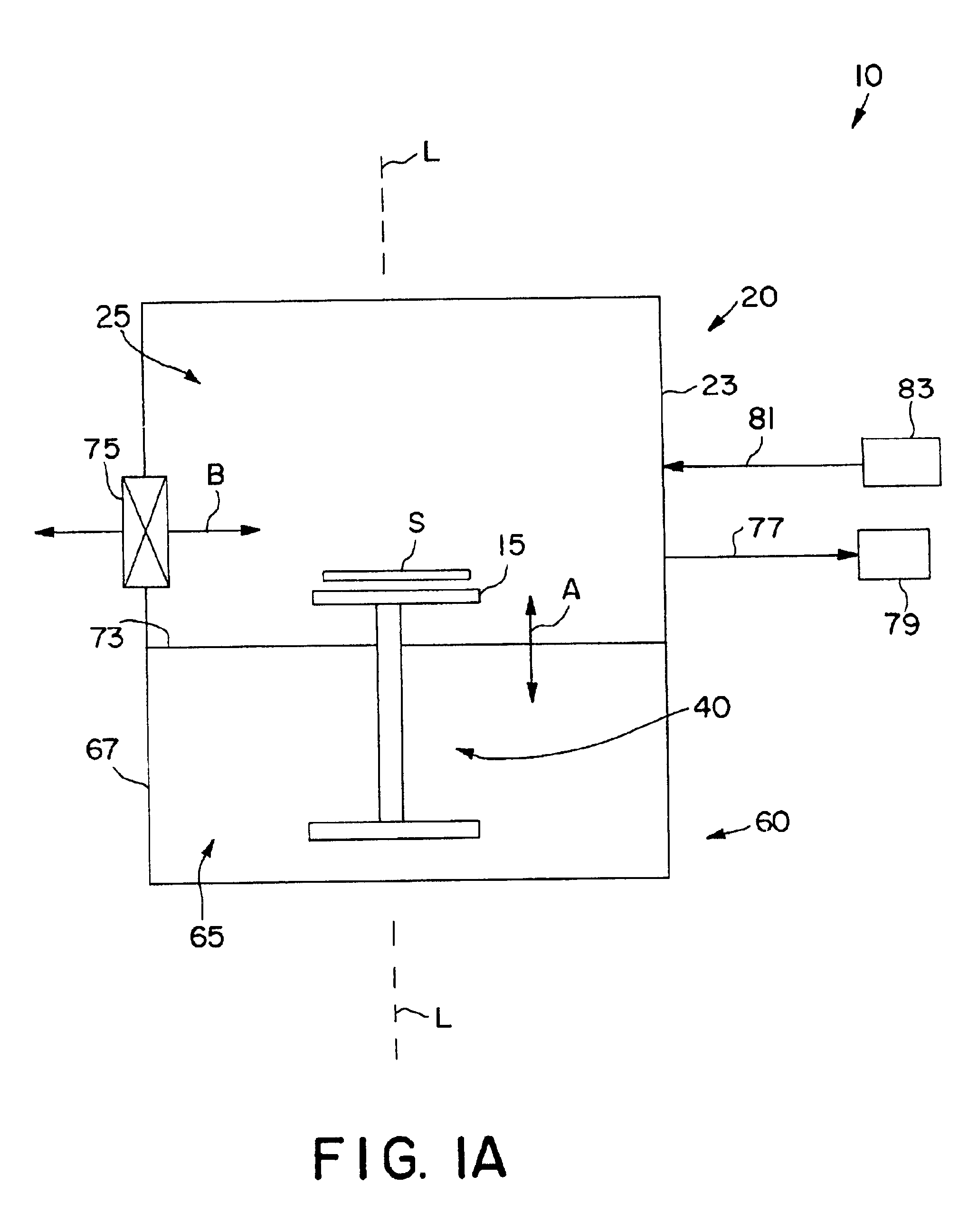
An apparatus and method for processing a microelectronic substrate comprises a main chamber and a movable boundary. The main chamber comprises a main chamber wall enclosing a main chamber interior. The movable boundary is disposed within the main chamber interior, and is movable between a first position and a second position. At the first position, the movable boundary at least partially defines a sub-chamber in which a substrate can be processed. The sub-chamber is fluidly isolated from the main chamber interior, and provides an environment suitable for a high-pressure processing of the substrate such as cleaning or surface preparation. The sub-chamber can be maintained at a high pressure while the main chamber is maintained at either a low pressure, an atmospheric pressure, or at a vacuum. The apparatus can be directly coupled to an external substrate handling and / or fabrication module, such that the main chamber interior provides a buffer between the sub-chamber and the external module. At the second position of the movable boundary, the substrate can be loaded into or removed from the apparatus, such as by transfer to or from any external module provided.

Description

TECHNICAL FIELD[0002]The present invention is generally related to the processing of substrates as part of, for example, a microscale device fabrication process. More particularly, the present invention relates to the processing (e.g., stripping, cleaning, drying, surface preparation, and the like) of substrates in a high-pressure environment that can be isolated from, yet functionally coupled with, an atmospheric or evacuated environment.BACKGROUND ART[0003]Microscale devices such as integrated circuits (ICs), optoelectronic, micromechanical, micro-electro-mechanical, and microfluidic devices contain micron- and sub-micron-sized features that are formed according to a precise sequence of fabrication steps and under tightly-controlled process conditions. Often a substrate such as a semiconductor wafer is provided, which contains active and passive electrical circuit elements such as transistors, resistors and capacitors. Semiconductor and thin-film deposition techniques are performe...

Claims


Application Information

Patent Timeline
IPC IPC(8): H01L21/3065B08B3/04B08B7/00H01L21/00H01L21/304
CPCB08B3/04B08B7/0021H01L21/67126H01L21/67751H01L21/68785Y10S414/135Y10S414/139
Inventor DICKINSON, C. JOHNJANSEN, FRANKMURPHY, DAIMHIN P.
Owner BOC EDWARDS
Learn More