
Define overlay dummy pattern in mark shielding region to reduce wafer scale error caused by metal deposition

a technology of shielding region and overlay, which is applied in the direction of microlithography exposure apparatus, instruments, photomechanical treatment, etc., can solve the problems of serious concerns about device performance and reliability, introduce measurement errors, etc., and achieve the effect of reducing the wafer scaling error

Inactive Publication Date: 2005-01-04
TAIWAN SEMICON MFG CO LTD
View PDF6 Cites 9 Cited by
  • Summary
  • Abstract
  • Description
  • Claims
  • Application Information

AI Technical Summary

Benefits of technology

In accordance with the objectives of the invention a new method is provided for the creation of a dummy pattern. A typical wafer exposure mask contains a Clear Out Window (CLWD) pattern, this CLWD pattern is of no value during the process of shielding the area on the surface of the wafer where the ali...

Problems solved by technology

A number of errors and inaccuracies-can be introduced during this exposure process, it is for instance of key importance that overlying layers of material that are to be processed are exactly aligned with each other since misalignment leads to serious concerns of device performance and reliability.
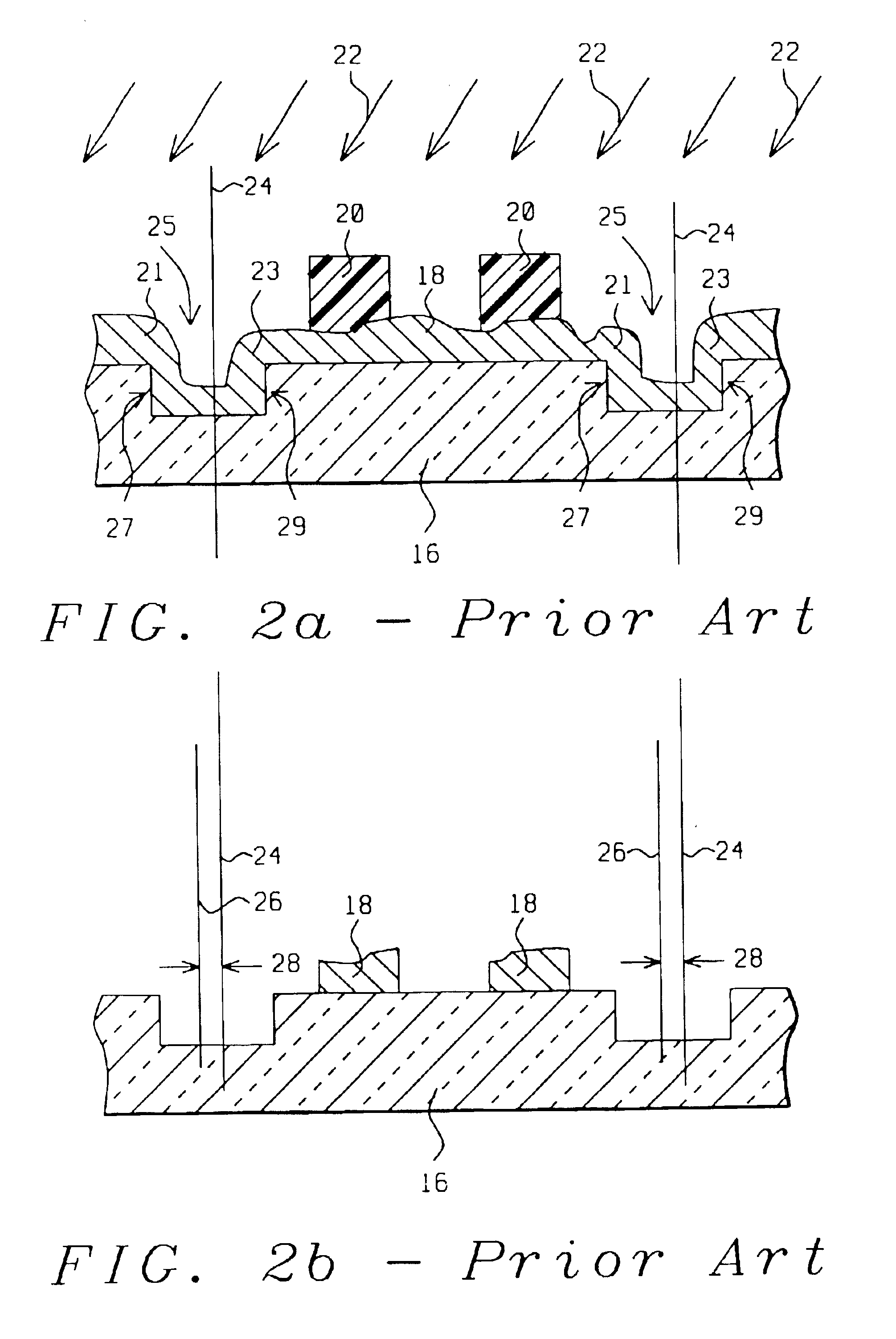
One of the problems that is encountered using the box-in-box technique is that asymmetric deposition of metal before an etch of one of the patterns of the box-in-box alignment marks introduces a measurement error.

Method used


Image

  • Define overlay dummy pattern in mark shielding region to reduce wafer scale error caused by metal deposition
  • Define overlay dummy pattern in mark shielding region to reduce wafer scale error caused by metal deposition
  • Define overlay dummy pattern in mark shielding region to reduce wafer scale error caused by metal deposition

Examples


Embodiment Construction

The reasons for wafer scale errors are first highlighted, using FIGS. 1a through 6b for this purpose.

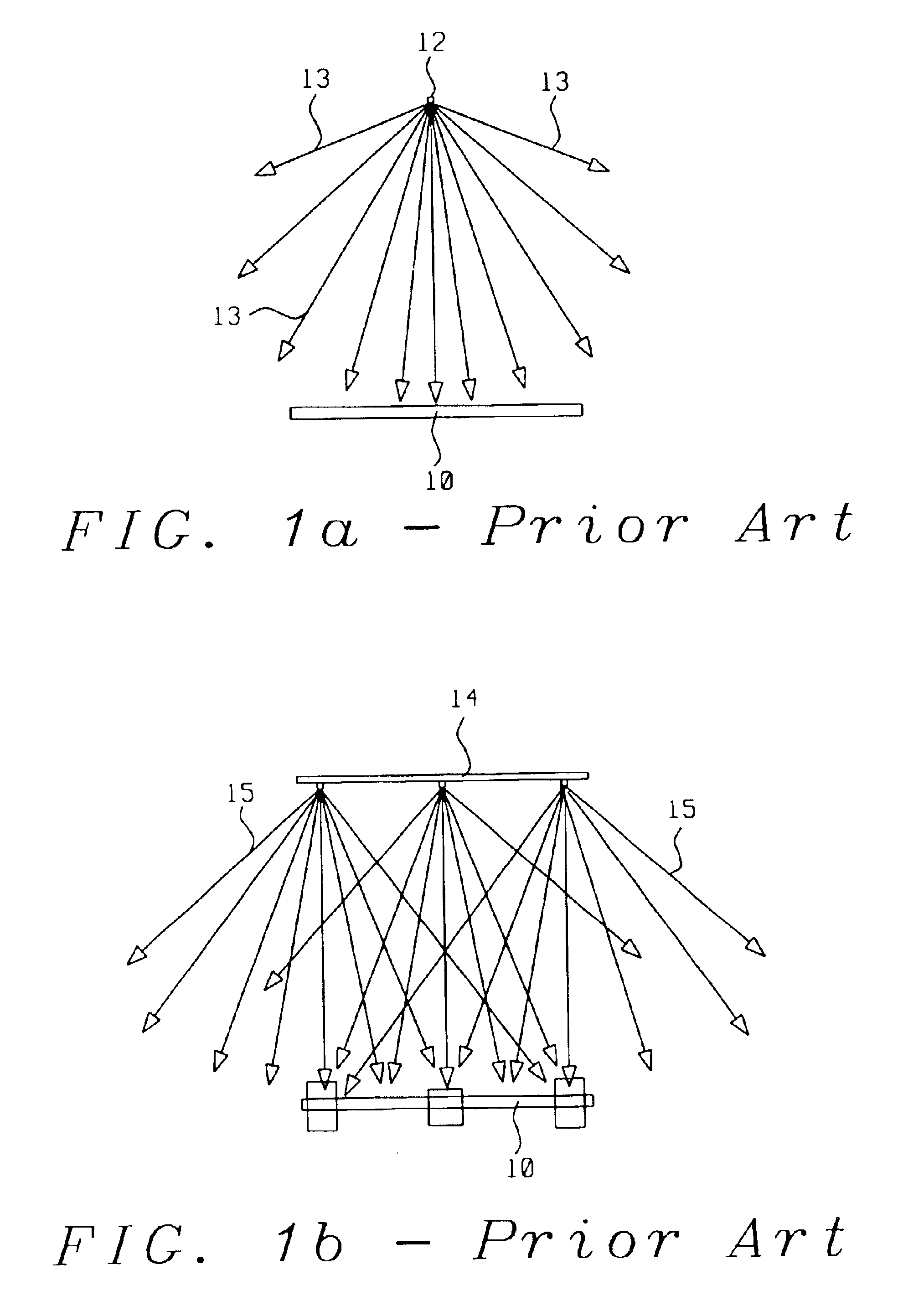
Referring now specifically to FIGS. 1a and 1b, there are shown two examples of exposure patterns whereby the exposure patterns originate from a source of different width or concentration. The example that is shown in FIG. 1a represents a source 12 of energy that is concentrated and can be considered a point of energy. The patterns of transmissions 13 and 15 that are shown in FIGS. 1a and 1b respectively can equally represent molecules of a semiconductor material such as metal that is sputter deposited on a semiconductor surface 10, such as the surface of a semiconductor substrate. Source 14 that is shown in FIG. 1b will be recognized as a distributed source of emission of radiated pattern 15.

Several observations can be made relating to the emission patterns that are shown in FIGS. 1a and 1b, as follows:the lines of propagation or flux lines 13 have a wide (distribution of) angle of e...


PUM


Abstract

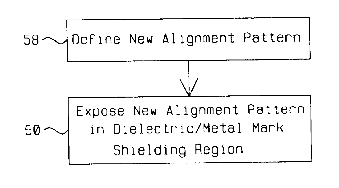
A new method is provided for the creation of a dummy pattern. A typical wafer exposure mask contains a Clear Out Window (CLWD) pattern, this CLWD pattern is of no value during the process of shielding the area on the surface of the wafer where the alignment mark must be placed. This CLWD can therefore be used to create a dummy overlay pattern, resulting in a reduction in the wafer scaling error that typically occurs as a result of metal deposition. For the same reasons, a dummy overlay pattern can also be created in the scribe lines of the wafer surface.

Description

BACKGROUND OF THE INVENTION(1) Field of the InventionThe invention relates to the fabrication of integrated circuit devices, and more particularly, to a method of eliminating errors in measuring overlay that are caused by metal deposition asymmetry before metal etching.(2) Description of the Prior ArtContinued emphasis on semiconductor device reduction has placed increased emphasis on the alignment of the overlying patterns that are required for the creation of a semiconductor device. Such patterns are typically created using a photolithographic process in which a pattern of the circuit is transferred from a microscopic scale onto the surface of a substrate where the pattern becomes part of a semiconductor device.In order to enhance device throughput, a typical photolithographic process uses a step-and-repeat function for the transfer of the pattern that is contained in the mask to the surface that is being exposed. A number of errors and inaccuracies-can be introduced during this e...

Claims


Application Information

Patent Timeline
IPC IPC(8): G03F7/20
CPCG03F7/70633
Inventor CHEN, YI-LINCHEN, SZU-PINGHSIEH, CHIN-CHUAN
Owner TAIWAN SEMICON MFG CO LTD
Learn More