Thermal displacement element and radiation detector using the element
a technology of radiation detector and element, which is applied in the direction of radiation controlled devices, instruments, optical radiation measurement, etc., can solve the problems of inability of infrared-ray detecting devices using conventional thermal displacement elements to accurately detect infrared-rays from targets, increasing costs, and inevitably increasing costs
- Summary
- Abstract
- Description
- Claims
- Application Information
AI Technical Summary
Benefits of technology
Problems solved by technology
Method used
Image
Examples
first embodiment
(First Embodiment)
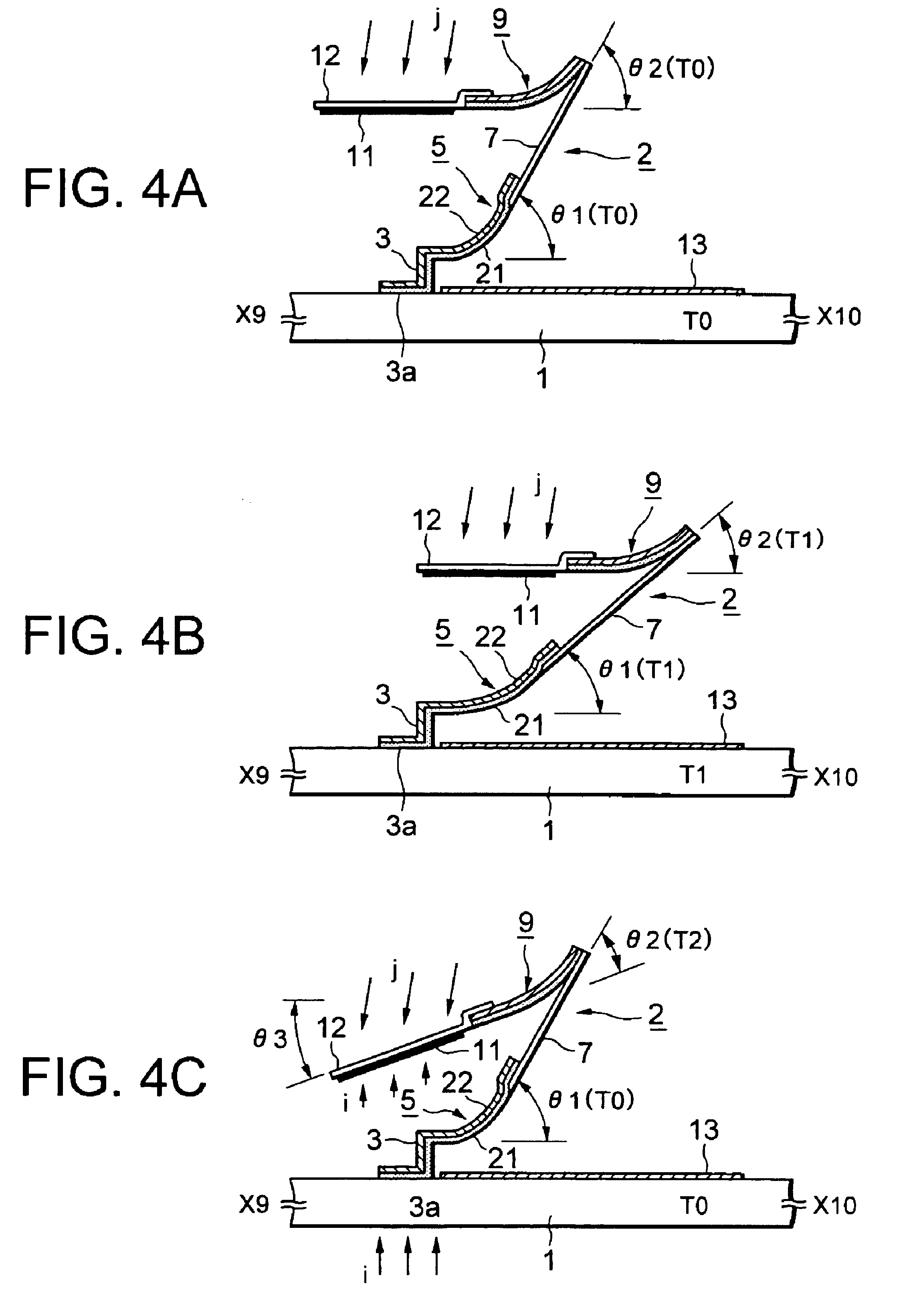
FIG. 1 is a schematic plan view schematically showing a unit pixel (unit element) of a radiation detecting device in a first embodiment of the present invention. FIG. 2 is a schematic sectional view taken along the line X1-X2 in FIG. 1. FIG. 3 is a schematic sectional view taken along the line X3-X4 in FIG. 1. FIGS. 1 through 3, however, show a state before a sacrifice layer 20 is removed in the process of manufacturing the radiation detecting device in this embodiment. This sacrifice layer 20 is illustrated in FIGS. 2 and 3 but is omitted in FIG. 1. Though not shown in the drawings, the schematic sectional view taken along the line X5-X6 in FIG. 1 is substantially the same as FIG. 3, and the schematic sectional view taken along the line X7-X8 in FIG. 1 is substantially the same as FIG. 4. Note that for explanatory convenience, as illustrated in FIG. 1, X-, Y- and Z-axes orthogonal to each other are defined, and a +X direction and a -X direction opposite to each ot...
second embodiment
(Second Embodiment)
FIG. 6 is a schematic plan view schematically showing the unit pixel of the radiation detecting device in a second embodiment of the present invention. FIG. 7 is a schematic sectional view taken along the line X11-X12 in FIG. 6. FIG. 8 is a schematic sectional view taken along the line X13-X14 in FIG. 6. FIG. 9 is a schematic sectional view taken along the line Y11-Y12 in FIG. 6. Referring to FIGS. 6 through 9, the elements that are the same as or correspond to the elements in FIGS. 1 through 4A-4C are marked with the same numerals, and the repetitive explanations thereof are omitted.
FIGS. 6 through 9 each shows a state before removing the sacrifice layer (unillustrated) in the process of manufacturing the radiation detecting device in this embodiment. Accordingly, in FIGS. 6 through 9, the first and second displacement portions 5, 6, 9, 10 are held by the sacrifice layer and not bent. Though not illustrated in the drawings, when the radiation detecting device in ...
third embodiment
(Third Embodiment)
FIG. 10 is a schematic plan view schematically showing the unit pixel of the radiation detecting device in a third embodiment of the present invention. FIG. 11 is a schematic sectional view taken along the line X15-X16 in FIG. 10. FIG. 12 is a schematic sectional view taken along the line Y15-Y16 in FIG. 10. Referring to FIGS. 10 through 12, the elements that are the same as or correspond to the elements in FIGS. 1 through 4A-4C are marked with the same numerals, and the repetitive explanations thereof are omitted.
FIGS. 10 through 12 each shows a state before removing the sacrifice layer (unillustrated) in the process of manufacturing the radiation detecting device in this embodiment. Accordingly, in FIGS. 10 through 12, the first and second displacement portions 5, 6, 9, 10 are held by the sacrifice layer and not bent. Though not illustrated in the drawings, when the radiation detecting device in this embodiment is completed by removing the sacrifice layer, as in ...
PUM
 Abstract
Description
Claims
Application Information
 - R&D
- Intellectual Property
- Life Sciences
- Materials
- Tech Scout
- Unparalleled Data Quality
- Higher Quality Content
- 60% Fewer Hallucinations
Browse by: Latest US Patents, China's latest patents, Technical Efficacy Thesaurus, Application Domain, Technology Topic, Popular Technical Reports.
© 2025 PatSnap. All rights reserved.Legal|Privacy policy|Modern Slavery Act Transparency Statement|Sitemap|About US| Contact US: help@patsnap.com


