
Electrical sensing apparatus and method utilizing an array of transducer elements

a transducer element and electric sensing technology, applied in the field of electric sensing apparatus and method utilizing an array of transducer elements, can solve the problems of limiting power consumption, noise and die area, increasing the speed at which data can be conveyed, and certain image sensor architectures consume a large amount of power

Inactive Publication Date: 2004-12-14
M RED INC
View PDF7 Cites 185 Cited by
  • Summary
  • Abstract
  • Description
  • Claims
  • Application Information

AI Technical Summary

Benefits of technology

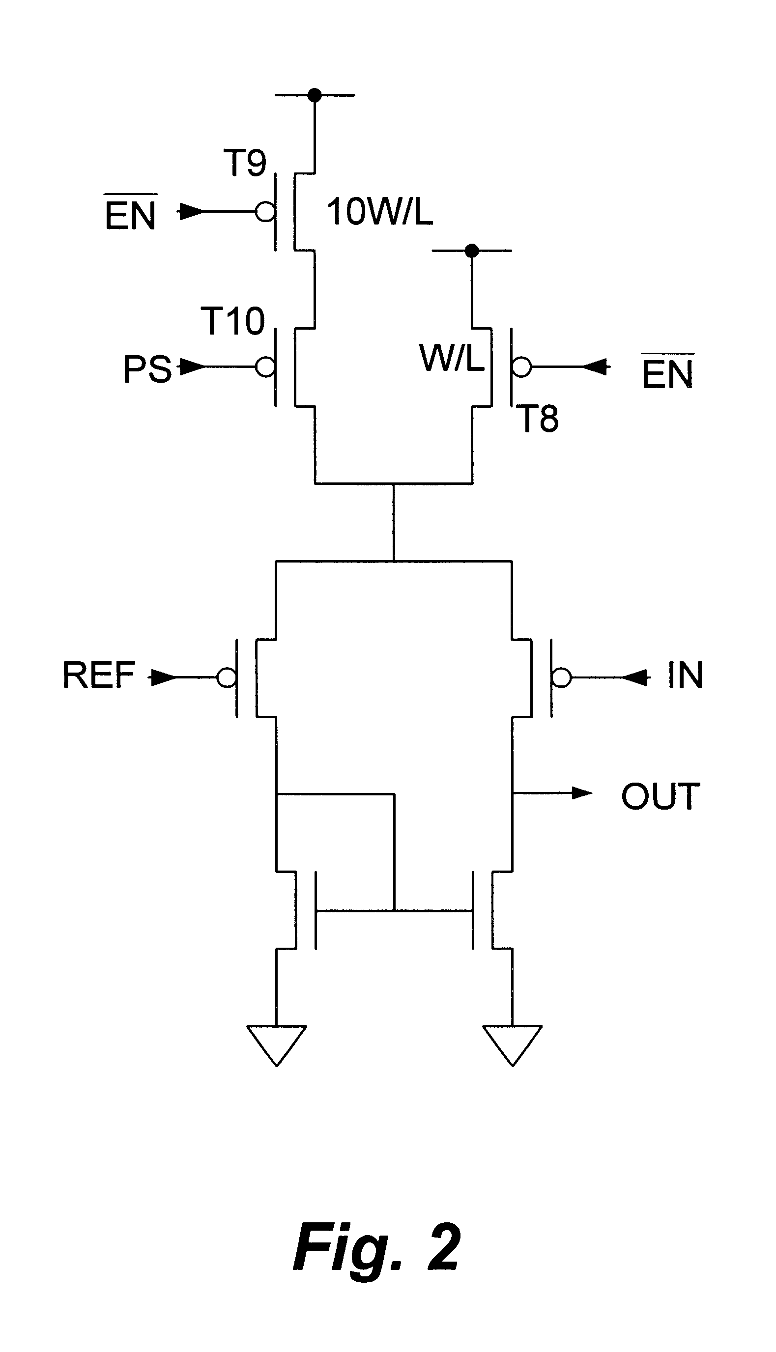
FIG. 2 is a circuit diagram of the first stage amplifier illustrating its a...

Problems solved by technology

There are a number of problems associated with this process mainly involving limiting power consumption, noise, and die area while increasing the speed at which data can be conveyed off chip.
Certain image sensor architectures consume a large amount of power.
The addition of features such as analog to digital converters (ADC) made feasible by CMOS image sensor technology only serves to increase the power consumption.
The high resolution and fast scanning rates of today's imagers also cause the speed of the output path to become a significant issue.
The large size of the array implies a need to drive long busses with large parasitic capacitances.
As well, the small pixel size results in the column amplifiers being confined to a narrow pitch, and therefore having a small current driving capability.
Solutions to these concerns do exist but they usually result in a large die area penalty.
If the die area occupied by the proposed solutions is too large, it will compromise the economic viability of the design.
Charge couple devices (CCD) and early CMOS image sensors did not integrate an ADC on chip.
Extra IC's are costly and inhibit the miniaturization of camera systems.
However, a single ADC places a significant bottleneck in the output path which needs to be addressed in order for fast pixel rates to be maintained.
The bottleneck issue becomes more prominent as array sizes continue to grow.
However, column parallel ADCs result in an extremely large die area penalty.
Column parallel ADCs also introduce a serious amount of noise to the system.
Not only is the amount of switching noise increased, but also column to column noise is introduced by process variations between the different ADCs.
Unfortunately, this technology results in a large pixel size and low fill factor which limit the possible resolution of the sensor.
As each pixel containing an ADC will logically consume more power than those that do not, arrays using pixel level ADC technology will be limited in size by their power consumption.

Method used


Image

  • Electrical sensing apparatus and method utilizing an array of transducer elements
  • Electrical sensing apparatus and method utilizing an array of transducer elements
  • Electrical sensing apparatus and method utilizing an array of transducer elements

Examples


Embodiment Construction

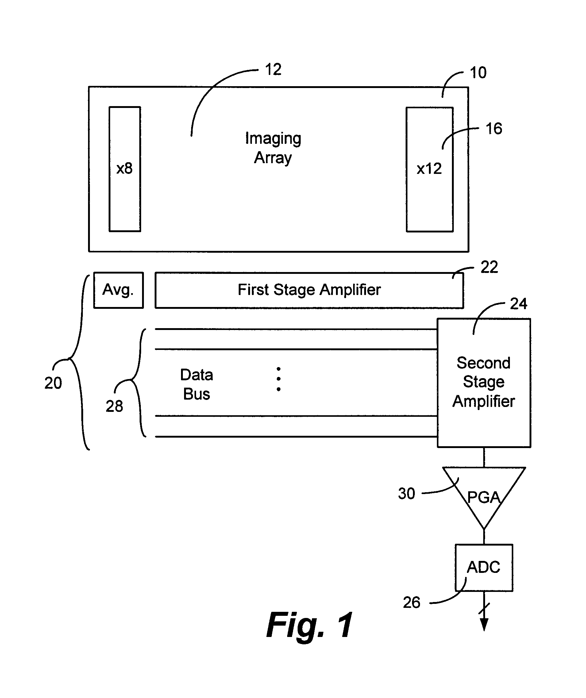
In one embodiment, a first stage amplifier exists for each column in the sensor array. These first stage amplifiers sample the data from the array while preferably having special noise and power reduction characteristics. The data is buffered by the first stage amplifiers until it is clocked onto a data bus in a pipeline fashion where it is sampled by the second stage amplifier. Each data line of the bus is coupled to an individual second stage amplifier. This second amplifier stage is not constrained by pitch and therefore can have a large drive capability. The second stage amplifiers will sequentially drive pixel data to the ADC while the others are sampling. Using this pipeline architecture, there will be a slight delay for the initial pixel data to reach the ADC but from that point on, a new pixel will arrive at the ADC with every clock cycle.

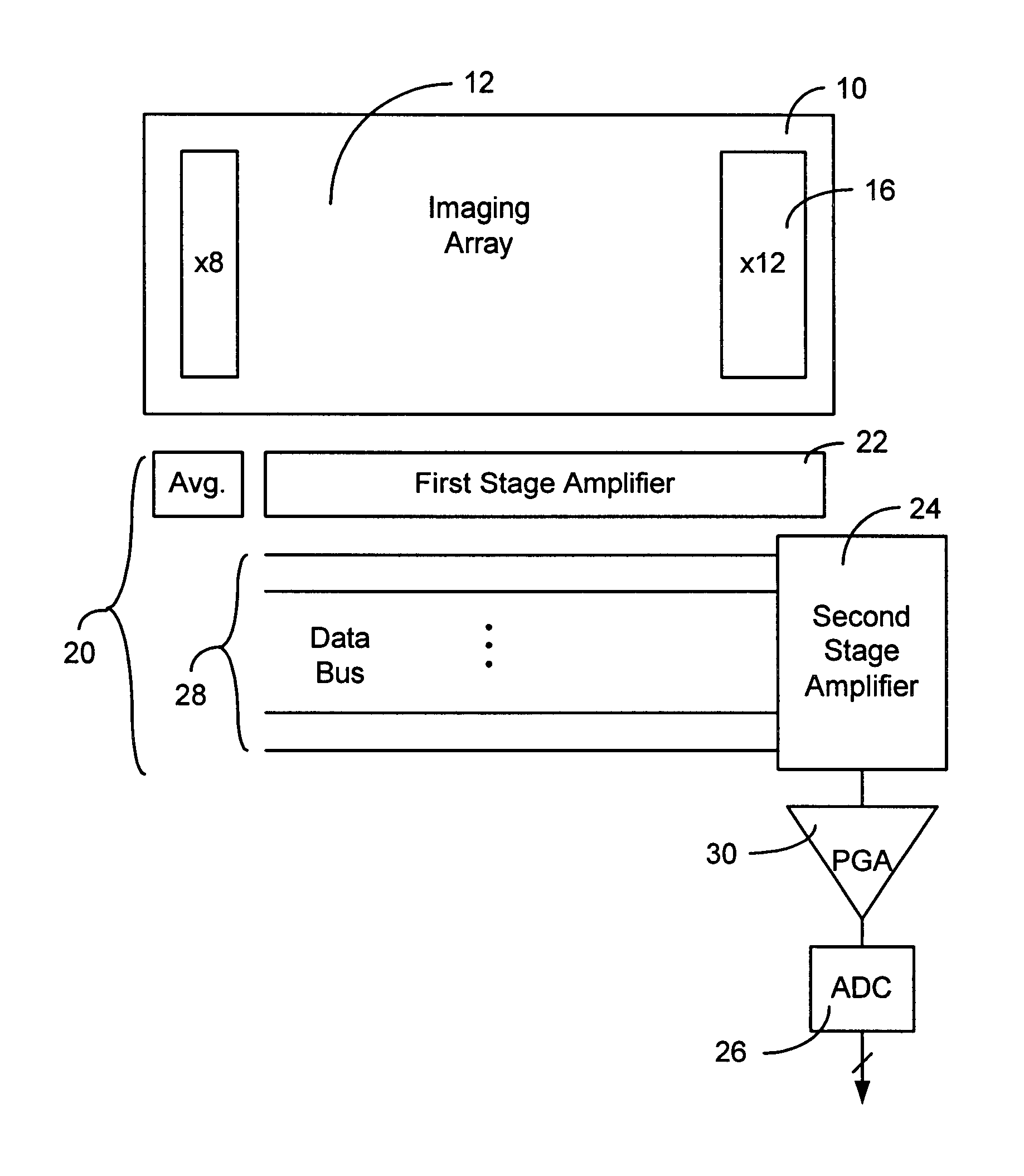
Referring to FIG. 1, there is shown a block diagram of the sensor array and analog output path according to an embodiment of the invention...


PUM


Abstract

Many electrical sensing devices include an array of transducer elements for converting external stimuli to electrical indications. Novel technologies to realize improvements in low power consumption, low noise, and analog output path which occupies minimal die area while maintaining certain data rates are disclosed. A two stage pipeline architecture of the invention in the analog output path maintains fast pixel rates with minimal ADC (analog digital converter) arrangement. A novel power supply and the use of differential amplifiers in connection with a black signal level as a reference voltage are also described.

Description

The invention generally relates to an electrical sensing apparatus and method utilizing an array of transducer elements. More particularly, it is directed to improvements in the analog output path of such an apparatus and method.BACKGROUND OF INVENTIONOne of the most common devices to include a sensor array is an image sensor, which has an array of pixels that convert optical signals into electrical analog signals. These analog signals must be transferred off chip, often after being converted into a digital signal. There are a number of problems associated with this process mainly involving limiting power consumption, noise, and die area while increasing the speed at which data can be conveyed off chip.In addition to image sensors which involve conversion between optical signals and electrical signals, there are a large number of different sensing elements which require conversion of signals from one type to another type. Some examples of these are elements dealing with acoustic wav...

Claims


Application Information

Patent Timeline
IPC IPC(8): H04N3/15H04N5/335G01J1/44G03B19/02
CPCH04N5/335H04N3/1512H04N25/00H04N25/633H04N25/78H04N25/63H04N25/75
Inventor JOHN, SCOTT-THOMASHUA, PAULCHAMBERLAIN, GEORGE
Owner M RED INC
Learn More