Feedforward amplifier circuitry
a technology of amplifier circuitry and feedforward, which is applied in the direction of amplifier modification to reduce non-linear distortion, digital transmission, and baseband system details, etc., and can solve problems such as lack of flexibility in location
- Summary
- Abstract
- Description
- Claims
- Application Information
AI Technical Summary
Benefits of technology
Problems solved by technology
Method used
Image

Examples
embodiment 1
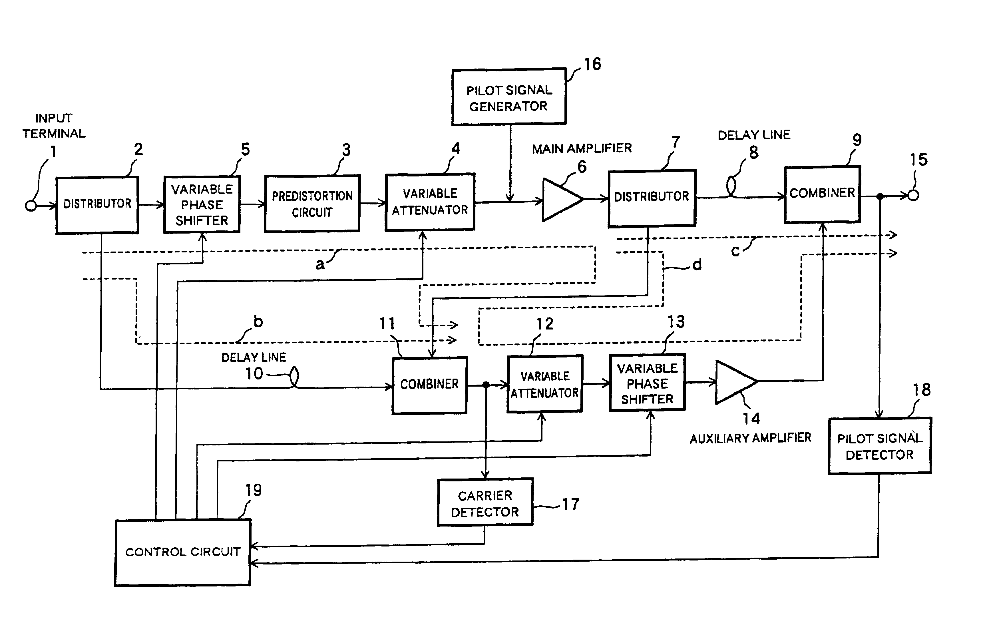
Hereinafter, a feedforward amplifier of an embodiment 1 according to the present invention will be described with reference to FIG. 1.
The feedforward amplifier circuitry as shown in FIG. 1 is a modified form of the feedforward amplifier circuitry of FIG. 9. In the feedforward amplifier circuitry of FIG. 1, an input signal from an input terminal 1 is distributed via a distributor 2 to signal paths a and b. The signal outputted on the signal path a passes through a variable phase shifter 5, a predistortion circuit (a pre-stage distortion compensating circuit) 3, a variable attenuator 4 and then receives an injection of a pilot signal generated from a pilot signal generator 16, thereafter inputted into a main amplifier 6.
An output from the main amplifier 6 is inputted into a distributor 7 and then distributed to signal paths c and d. A signal outputted on the signal path c is fed through a delay line 8 into a combiner 9 while a signal outputted on the signal path d is inputted into a c...
embodiment 2
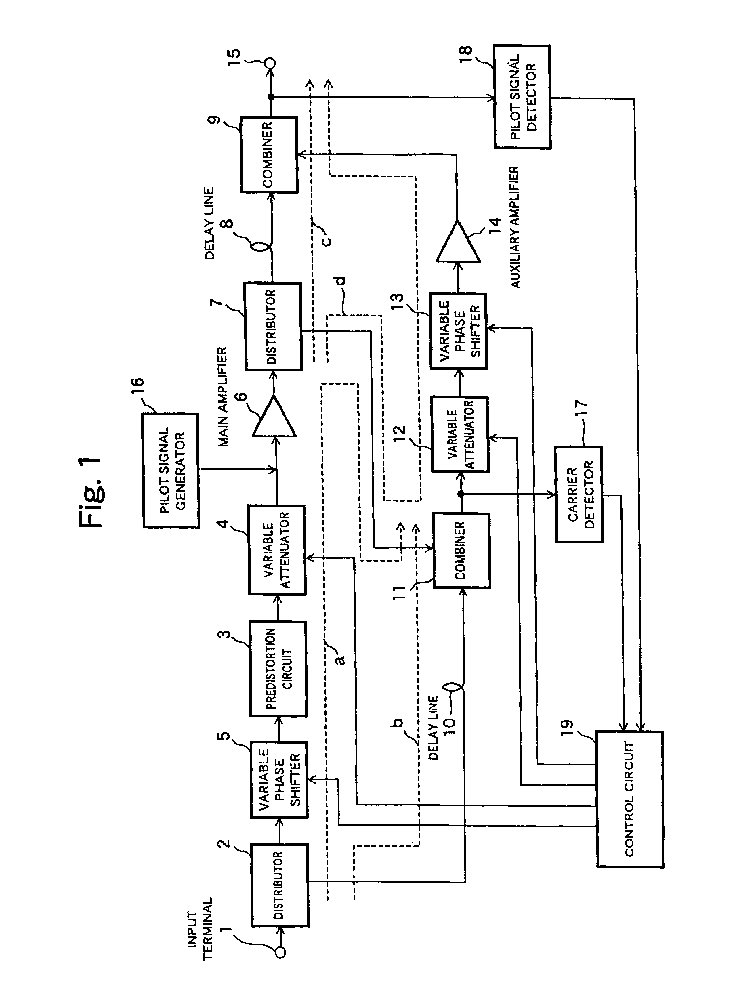
Next, a feedforward amplifier circuitry of an embodiment 2 according to the present invention will be described with reference to FIG. 2. In comparison with the feed forward amplifier circuitry of FIG. 9, the feedforward amplifier circuit of FIG. 2 is different therefrom in that a variable phase shifter 5 in the feedforward amplifier of FIG. 2 is not disposed on a signal path a but is disposed on a signal path b. Accordingly, a control circuit 19 of FIG. 2 controls the variable phase shifter 5 such that a signal on the signal path a becomes opposite in phase to a signal on the signal path b. The feedforward amplifier circuitry of FIG. 2 is identical in performance to that of FIG. 9. In this embodiment 2, it is possible to relocate or move a variable phase shifter 13 from a location as shown in FIG. 2 to a location between a distributor 7 and a delay line 8.
embodiment 3
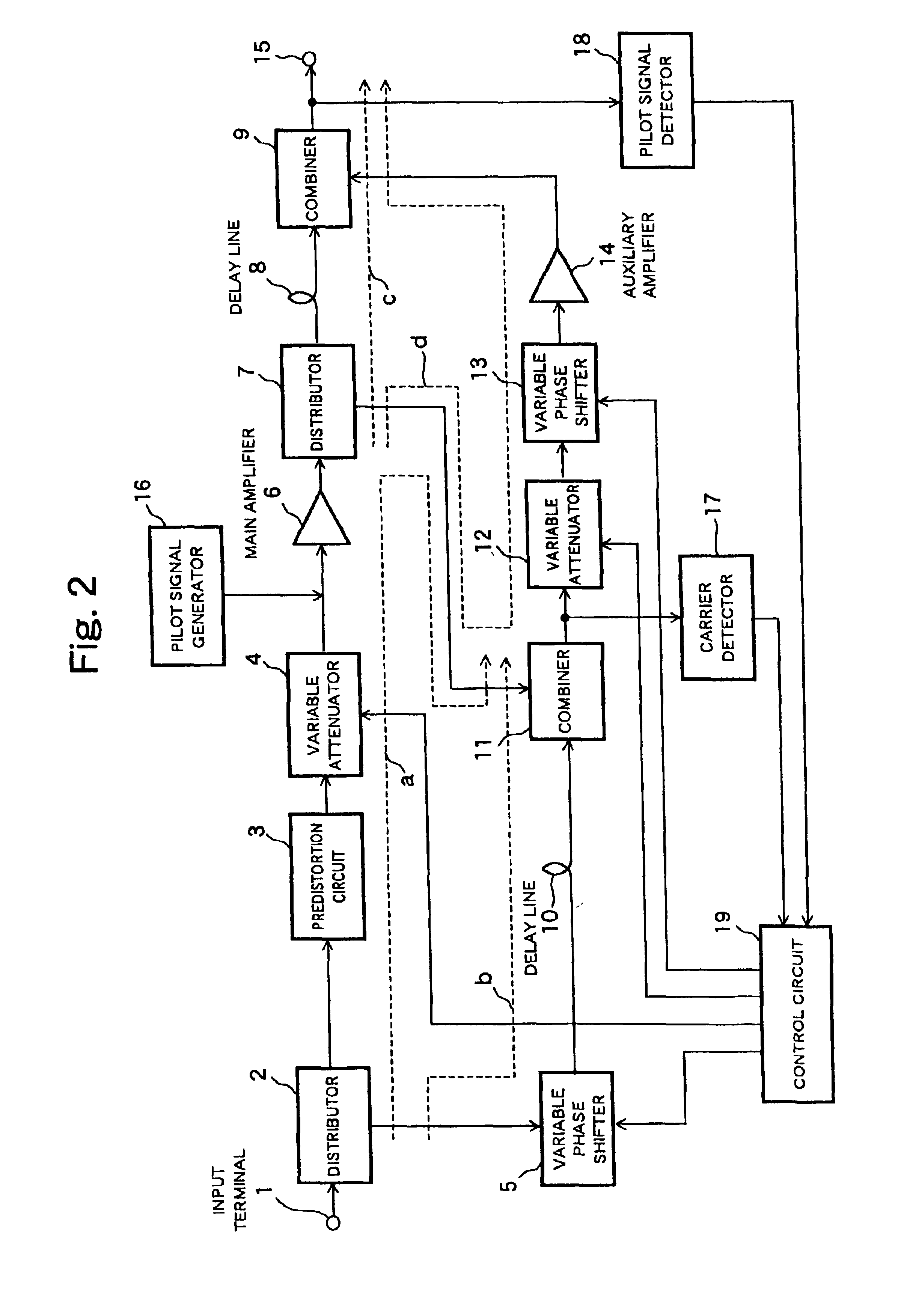
Next, a feedforward amplifier circuitry of an embodiment 3 according to the present invention will be described with reference to FIG. 3.. In comparison with the feed forward amplifier circuitry of FIG. 10, the feedforward amplifier circuit of FIG. 3 is different therefrom in that a variable phase shifter 5 on a signal path a as shown in FIG. 3 is not disposed on a post-stage of a predistortion circuit 3 but is disposed on a pre-stage of the predistortion circuit 3. Also, in comparison with the feedforward amplifier circuitry of FIG. 10, the feedforward amplifier circuit of FIG. 3 is different therefrom in that a variable phase shifter 13 on a signal path d as shown in FIG. 3 is not disposed on a post-stage of a predistortion circuit 20 but is disposed on a pre-stage of the predistortion circuit 20. Accordingly, although each location of the variable shifters 5 and 13 in the feedforward amplifier of FIG. 3 is different from the corresponding one in the feedforward amplifier circuitr...
PUM
 Abstract
Description
Claims
Application Information
 - R&D
- Intellectual Property
- Life Sciences
- Materials
- Tech Scout
- Unparalleled Data Quality
- Higher Quality Content
- 60% Fewer Hallucinations
Browse by: Latest US Patents, China's latest patents, Technical Efficacy Thesaurus, Application Domain, Technology Topic, Popular Technical Reports.
© 2025 PatSnap. All rights reserved.Legal|Privacy policy|Modern Slavery Act Transparency Statement|Sitemap|About US| Contact US: help@patsnap.com