Bus hold circuit with power-down and over-voltage tolerance

Active Publication Date: 2004-08-10
SEMICON COMPONENTS IND LLC
View PDF8 Cites 14 Cited by
  • Summary
  • Abstract
  • Description
  • Claims
  • Application Information

AI Technical Summary

Benefits of technology

U.S. Pat. No. 6,150,845 to Morrill (Morrill), which is commonly owned with the present application, describes a bus hold circuit with both power-down, over-voltage tolerance, and that prevents leakage from the input / output pins. But, the circuit undesirably contains many devices and consumes DC power in order to sense the over-voltage occurrence.
It is an objective of the present invention to provide a bus hold circuit for use in computer, communications, interfacing and generally in virtually any digital system where symmetrical operation is desirable, and where such digital systems exhibit: power-down and over-voltage tolerance; economy of devices; and virtually no DC power consumption.
The invention provides a CMOS inverter with a latching feedback inverter that includes a first PMOS device that selectively powers the second inverter. The N-well of this first PMOS device is connected to a pseudo power rail or prail. An arbiter circuit connects the more positive of the input voltage or the Vcc to the prail. This arrangement prevents the drain to N-well junction of this first PMOS device from becoming forward biased if Vin exceeds Vcc.
The comparator circuit, the first PMOS device, and the second PMOS switch acting together with the entire bus hold circuitry reduce the window of uncertainty between Vcc and Vin to about 100 millivolts.

Problems solved by technology

Older bus hold circuits have neither power-down nor over-voltage tolerance and faulty or unacceptable conditions may occur under such circumstances.
In such occurrences, leakage currents may unacceptably load the input signal.
This 1.2V range is unacceptable.
But, the circuit undesirably contains many devices and consumes DC power in order to sense the over-voltage occurrence.

Method used


Image

  • Bus hold circuit with power-down and over-voltage tolerance
  • Bus hold circuit with power-down and over-voltage tolerance
  • Bus hold circuit with power-down and over-voltage tolerance

Examples


Embodiment Construction

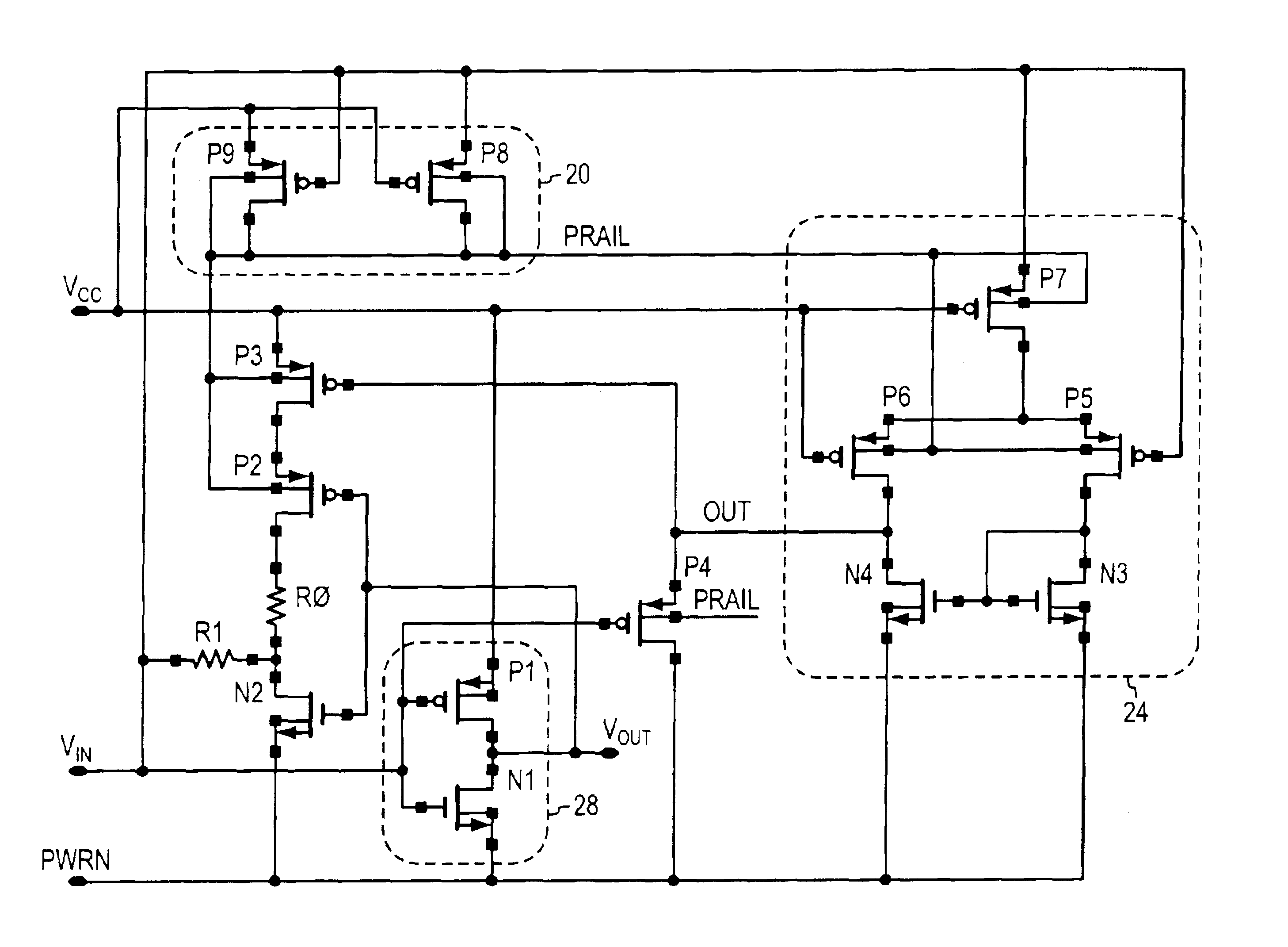
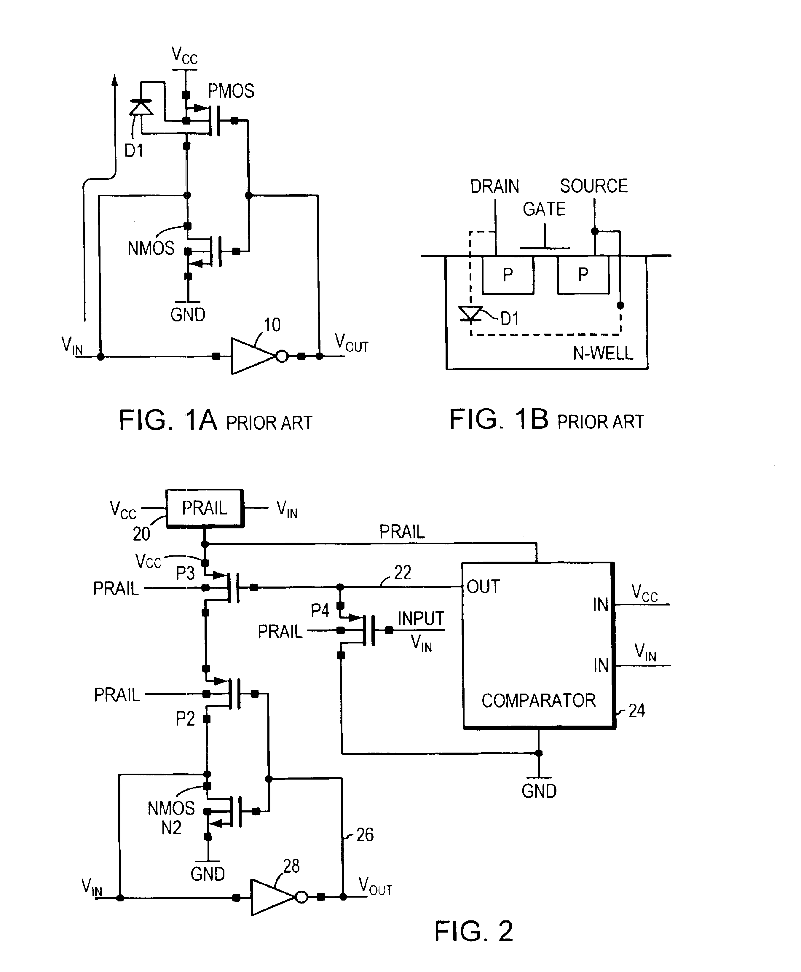
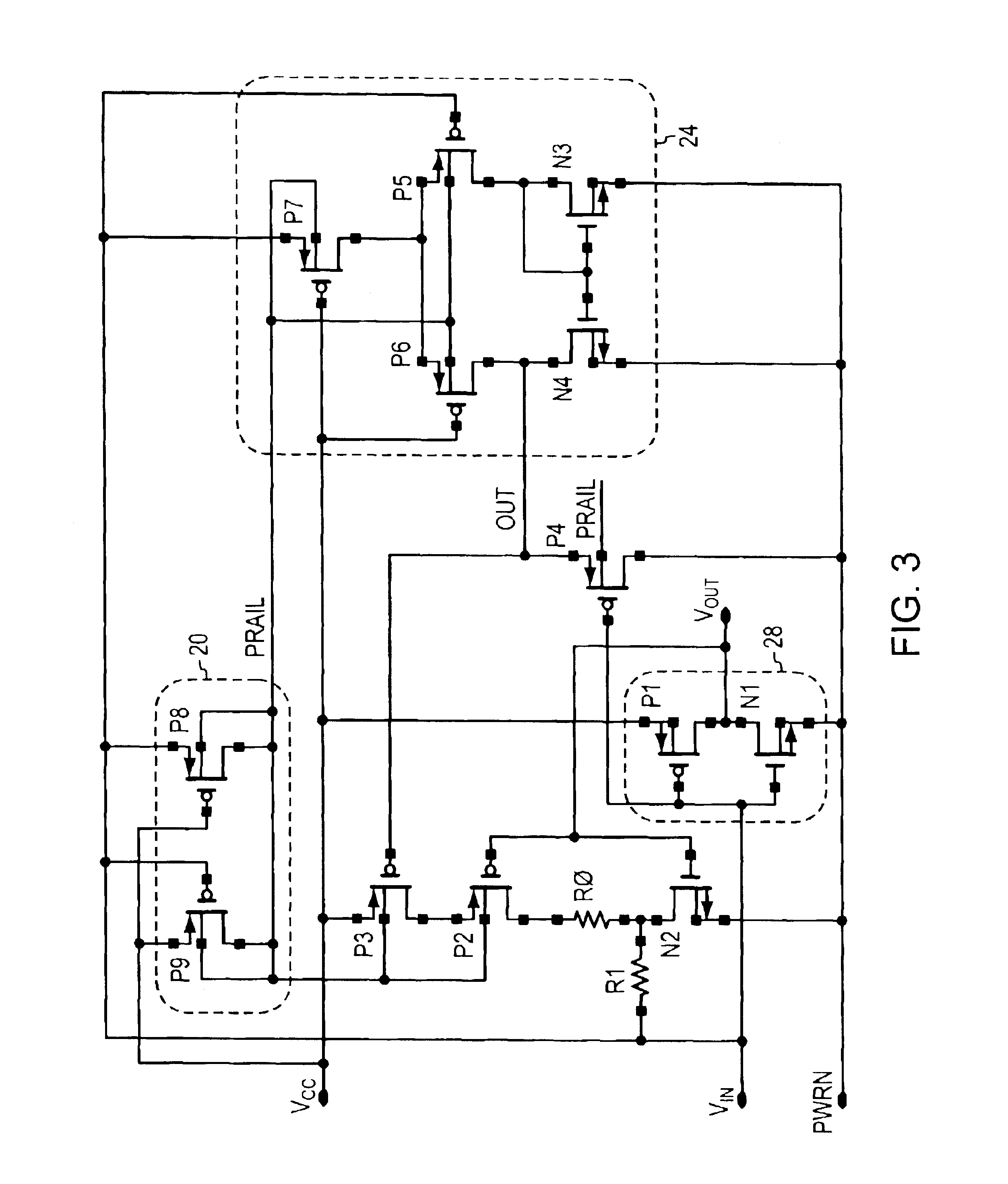
. 2 in block form illustrates the approach of the present invention. In this circuit a separate power connection, referred to as a prail, is arranged to power part of the circuitry of the bus hold with the higher of Vin or Vcc as determined from the prail arbiter circuit 20 as discussed below. In this block diagram P3 connects Vcc to the latching inverter made up of N2 and P2. When Vin exceeds Vcc, P3 is turned off and prevents leakage current from flowing from Vin to Vcc as described with respect to FIG. 1A. Notice that the prail provides power only to the N-wells of the PMOS transistors which removes the leakage path from Vin to Vcc when Vin is larger than Vcc.

With respect to FIG. 2, three conditions are examined:

First, the "normal" condition when Vin is at a logic low. In this condition Vcc appears on the prail through the arbiter circuit 20; P4 is turned on driving the gate of P3 low turning it on. Vcc powers the feedback inverter comprising P2 and N2 via the source of P2. Under...


PUM


Abstract

A bus hold circuit of CMOS components that draws no DC current and is over voltage tolerant is described. No leakage current is drawn from the input when the input voltage is greater than the bus hold circuit supply voltage. A feedback inverter is used to s latch the Vin logic in the bus hold circuit. When Vin is low, it turns on a first switch that drives the gate of a PMOS switch low turning it on. The PMOS switch connects the power connection of the feedback inverter to Vcc. The gate remains low, keeping the PMOS switch turned on as Vin increases. The first switch is turned off, but the gate of the PMOS switch remains low, until Vin exceeds Vcc. At that point, a comparator drives the gate of the PMOS to Vin shutting the PMOS switch off. An arbiter circuit selects the higher of Vcc and Vin to bias the N-well of the PMOS switch and other PMOS components in the comparator and arbiter circuit. This biasing ensures that the N-wells are never forward biased, thereby preventing leakage from the Vin.

Description

1. Field of the InventionThe present invention relates to bus driver circuits and more particularly to bus hold circuits that maintain the output logic state when the source of the input signal assumes a high impedance state; and more particularly to CMOS bus hold circuitry that is over voltage tolerant, that does not create a leakage path when powered down, and is frugal of DC power and components.2. Background InformationTraditional bus hold circuits latch data from an input connection while providing a high impedance load on the input connection. Older bus hold circuits have neither power-down nor over-voltage tolerance and faulty or unacceptable conditions may occur under such circumstances. Over voltage will occur when, for example, a +5 volt logic system interfaces with a +3.3 V system, or transiently when severe input signal over-shoots occur. Power down situations happen when a portion of a system is unpowered, say for maintenance purposes, or to conserve battery life. In su...

Claims


Application Information

Patent Timeline
IPC IPC(8): H03K3/356H03K3/00
CPCH03K3/35613H03K3/356165H03K2217/0018H03K3/00H03K3/356G06F13/00G06F1/32
Inventor MISKE, MYRON J.LOMBARD, STEPHEN B.
Owner SEMICON COMPONENTS IND LLC
Why Eureka
Try Eureka