
Phosphor multilayer and EL panel

Inactive Publication Date: 2004-07-13
IFIRE IP CORP
View PDF20 Cites 3 Cited by
  • Summary
  • Abstract
  • Description
  • Claims
  • Application Information

AI Technical Summary

Problems solved by technology

Thin-film EL displays using sulfide phosphor thin films are fully reliable and resistant to environment, but at present regarded unsuitable as color displays because EL phosphors required to emit light in the primaries of red, green and blue have poor characteristics.
These phosphor thin films capable of emitting light in the primaries of red, green and blue suffer from problems of emission luminance, emission efficiency and color purity.
Thus color EL panels have not reached the commercial stage.
However, its luminance is still short as the blue color for full-color displays and its chromaticity is shifted toward green.
These thiogallate base phosphors are satisfactory in color purity, but suffer from a low luminance and especially, difficulty to form a thin film of uniform composition because of the multi-component composition.
It is believed that thin films of quality are not obtainable because of poor crystallinity resulting from inconvenient composition control, formation of defects resulting from sulfur removal, and admittance of impurities; and these factors lead to a failure to increase the luminance.
In particular, thioaluminate base phosphors are quite difficult to control their composition.
Since the spectrum of light emission consists of bright lines, this thin film develops a thin film interference effect.
There still remain problems of visual angle dependency and a low luminance.
This is probably because alkaline earth aluminates are difficult to form crystalline thin films and thus cannot be utilized as phosphor thin films capable of electroluminescent light emission.
EL devices were prepared using the thin films, but they failed to produce the desired light emission.
However, too thick a film requires an increased EL drive voltage whereas too thin a film results in a low emission efficiency.
If the substrate temperature is too high, the thin film of matrix material may have more asperities on its surface and contain pin holes therein, giving rise to the problem of current leakage on EL devices.
If the pressure exceeds the range, the operation of the electron gun becomes unstable, and composition control becomes very difficult.
If the rotational speed of the substrate is too high, there may arise a problem of seal upon admission into the vacuum chamber.
If the rotational speed of the substrate is too low, compositional gradation may occur in the thickness direction within the chamber so that the characteristics of the light emitting layer may become poor.

Method used


Image

  • Phosphor multilayer and EL panel
  • Phosphor multilayer and EL panel
  • Phosphor multilayer and EL panel

Examples


example 1

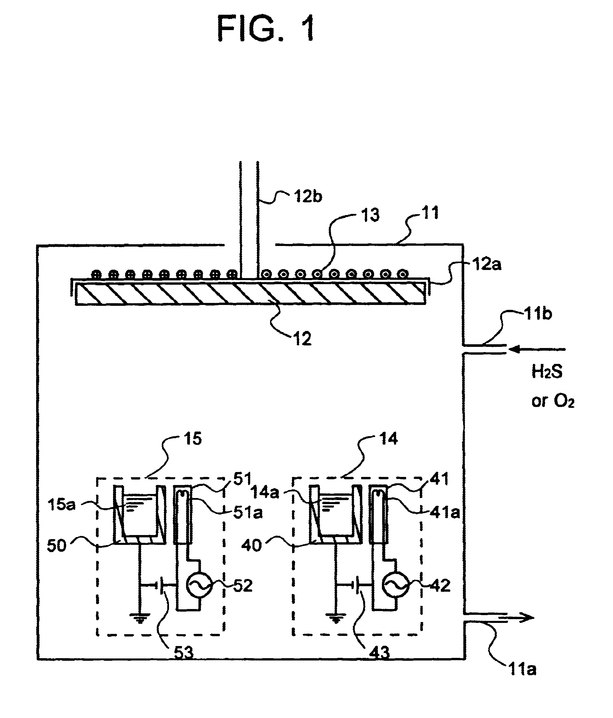
FIG. 1 illustrates an exemplary evaporation chamber which can be used in the manufacturing method of the invention. One electron gun and one resistive heating cell were used instead of a two-point controlled electron gun.

An EB source 15 containing BaS powder having 5 mol % of Eu added and a resistive heating cell (14) containing Al.sub.2 S.sub.3 powder were placed in a vacuum chamber 11. The substances were simultaneously evaporated from the respective sources, and deposited on a rotating substrate heated at 400.degree. C., forming a Ba.sub.x Al.sub.y O.sub.z S.sub.w :Eu layer. The rates of evaporation from the respective sources were adjusted so that the film was deposited on the substrate at a deposition rate of 1 nm / sec. During evaporation, H.sub.2 S gas was admitted at 20 SCCM. The thin film formation was followed by annealing at 750.degree. C. for 10 minutes in air, yielding the first thin film of 300 nm thick.

By an EB evaporation technique using a ZnS pellet having 0.5 mol % o...


PUM


Abstract

The invention aims to provide a phosphor multilayer eliminating a need for filters, having a satisfactory color purity and useful in white monochromatic EL devices, and an EL panel. Such objects are achieved by a phosphor multilayer comprising at least a first thin film and a second thin film wherein the first thin film is formed of a matrix material comprising barium aluminate as a main component, containing sulfur element and further containing Eu as a luminescent center, and the second thin film is formed of a matrix material comprising zinc sulfide as a main component, and an EL panel using the same.

Description

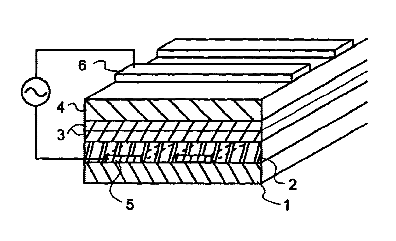
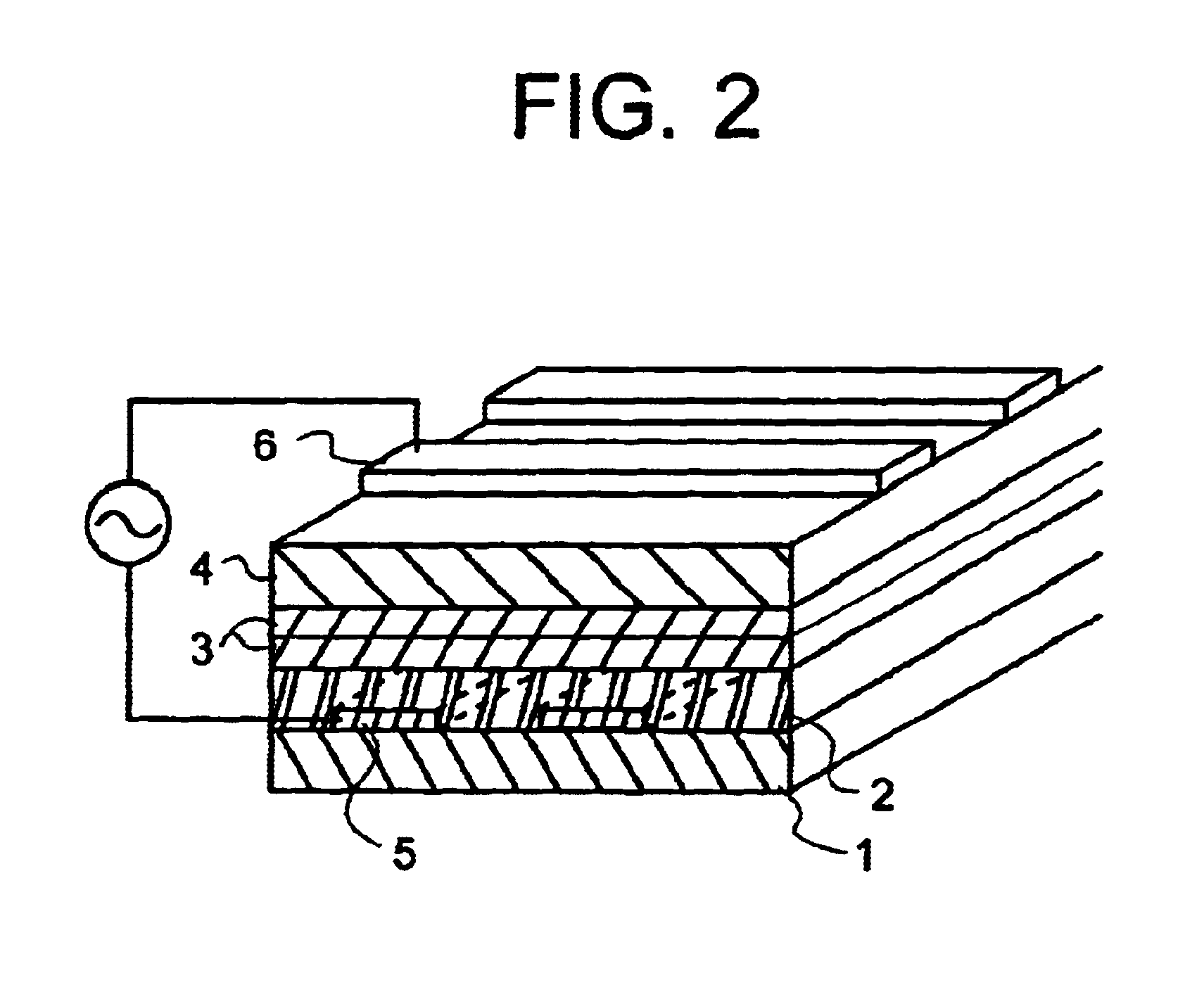
1. Technical FieldThis invention relates to a light-emitting layer for use in inorganic EL devices, and more particularly, to a white light emitting multilayer of phosphor thin films and an EL panel using the same.2. Background ArtIn the recent years, active research works have been made on thin-film EL devices as small-size and large-size, lightweight flat displays. A monochromatic thin-film EL display using a phosphor thin film of manganese-doped zinc sulfide capable of emitting yellowish orange light has already become commercially practical as a dual insulated structure using thin-film insulating layers 2 and 4 as shown in FIG. 2. In FIG. 2, a predetermined pattern of lower electrodes 5 is formed on a substrate 1, and a first insulating layer 2 is formed on the lower electrodes 5. On the first insulating layer 2, a light-emitting layer 3 and a second insulating layer 4 are successively formed. On the second insulating layer 4, a predetermined pattern of upper electrodes 6 is for...

Claims


Application Information

Patent Timeline
IPC IPC(8): C09K11/77H05B33/14C09K11/80
CPCC09K11/7734H05B33/14
Inventor YANO, YOSHIHIKONAGANO, KATSUTO
Owner IFIRE IP CORP
Learn More