
Carbon nanotube with a graphitic outer layer: process and application

a carbon nanotube and graphitic outer layer technology, applied in the field of process and application, can solve the problems of low yield of prior art carbon nanotube production methods, silicon nitride pyramid-tip scanning probe microscope cannot meet the requirements of the semiconductor industry,

Inactive Publication Date: 2003-06-24
CENT FLORIDA UNIV OF
View PDF19 Cites 70 Cited by
  • Summary
  • Abstract
  • Description
  • Claims
  • Application Information

AI Technical Summary

Benefits of technology

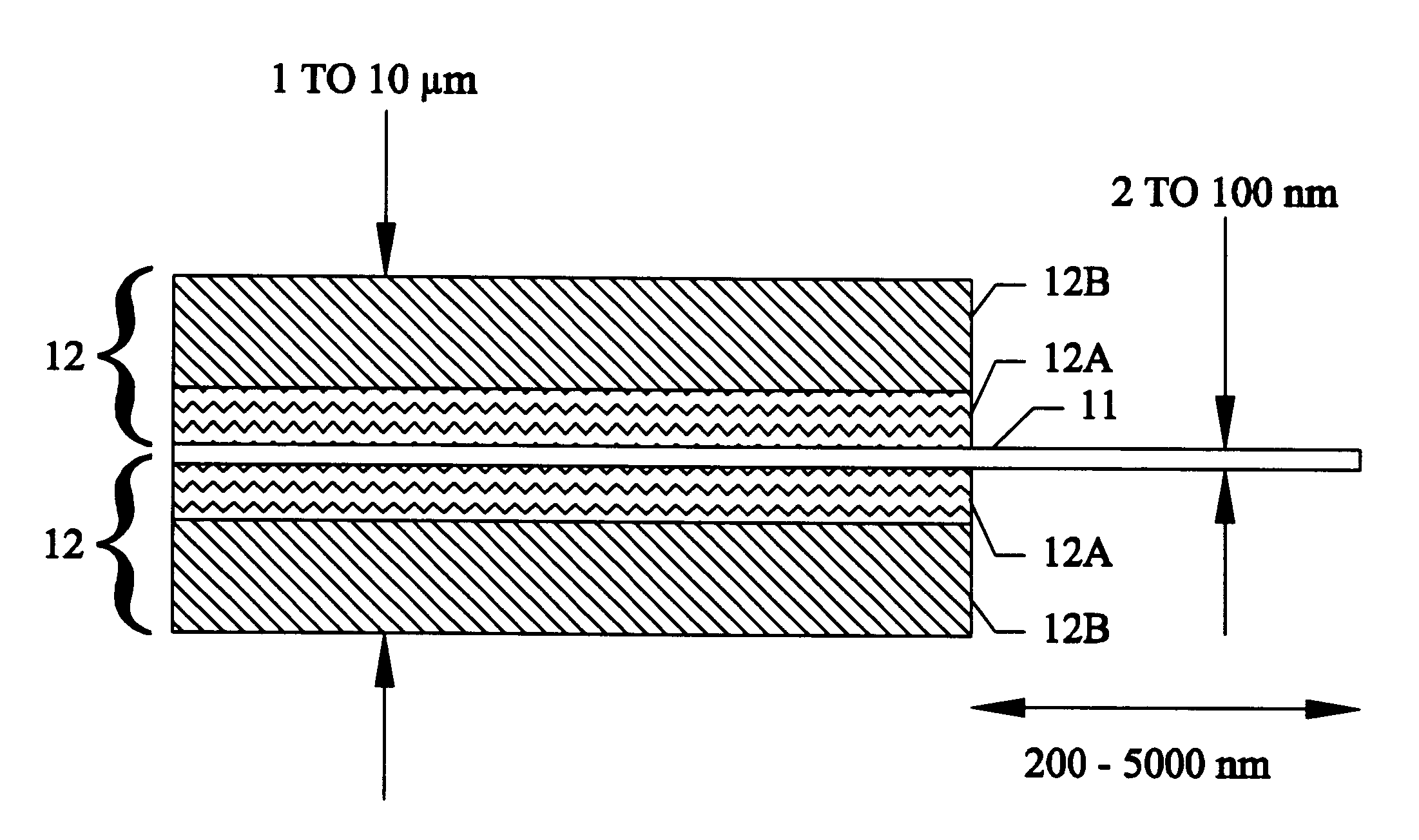
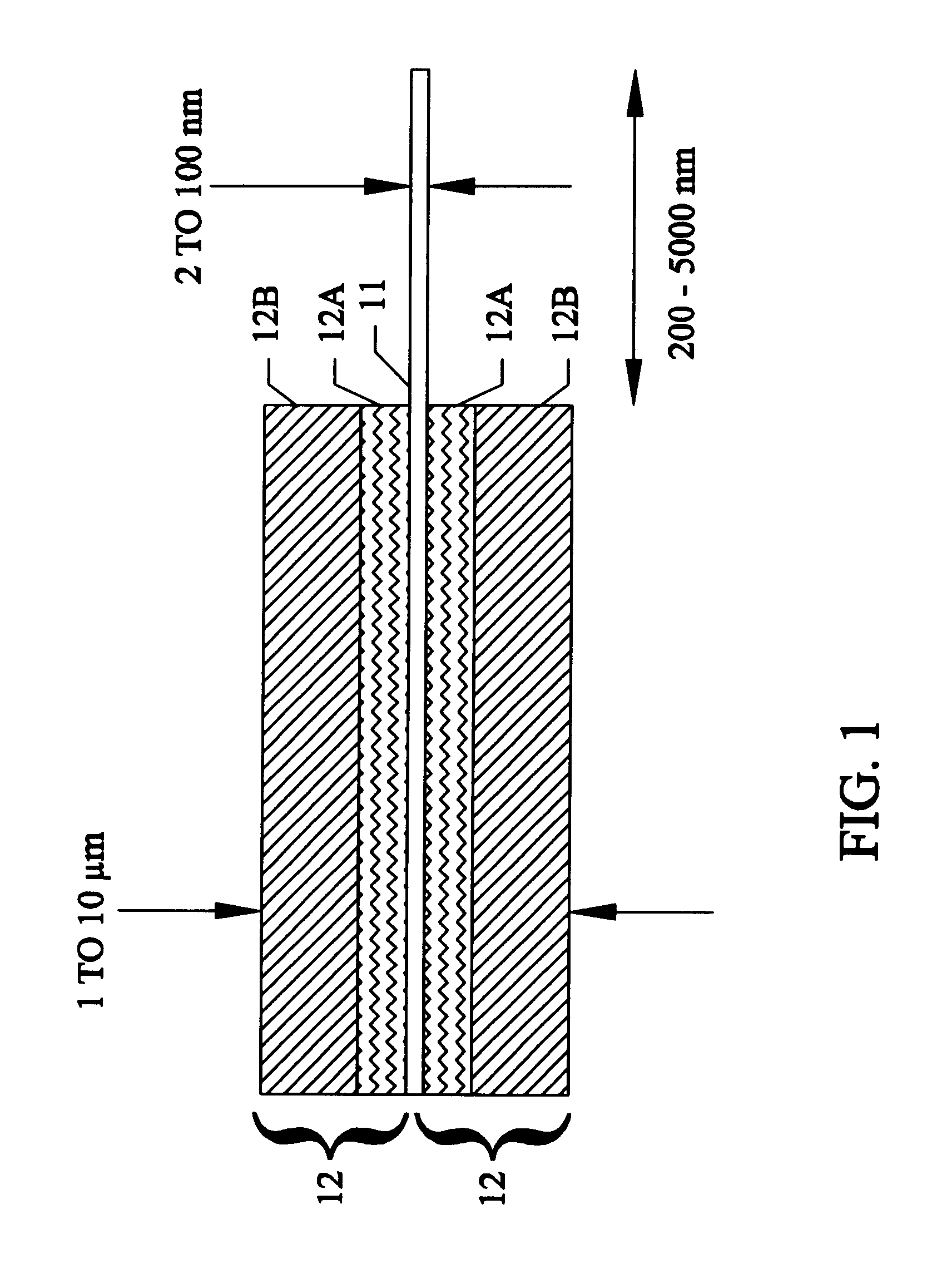
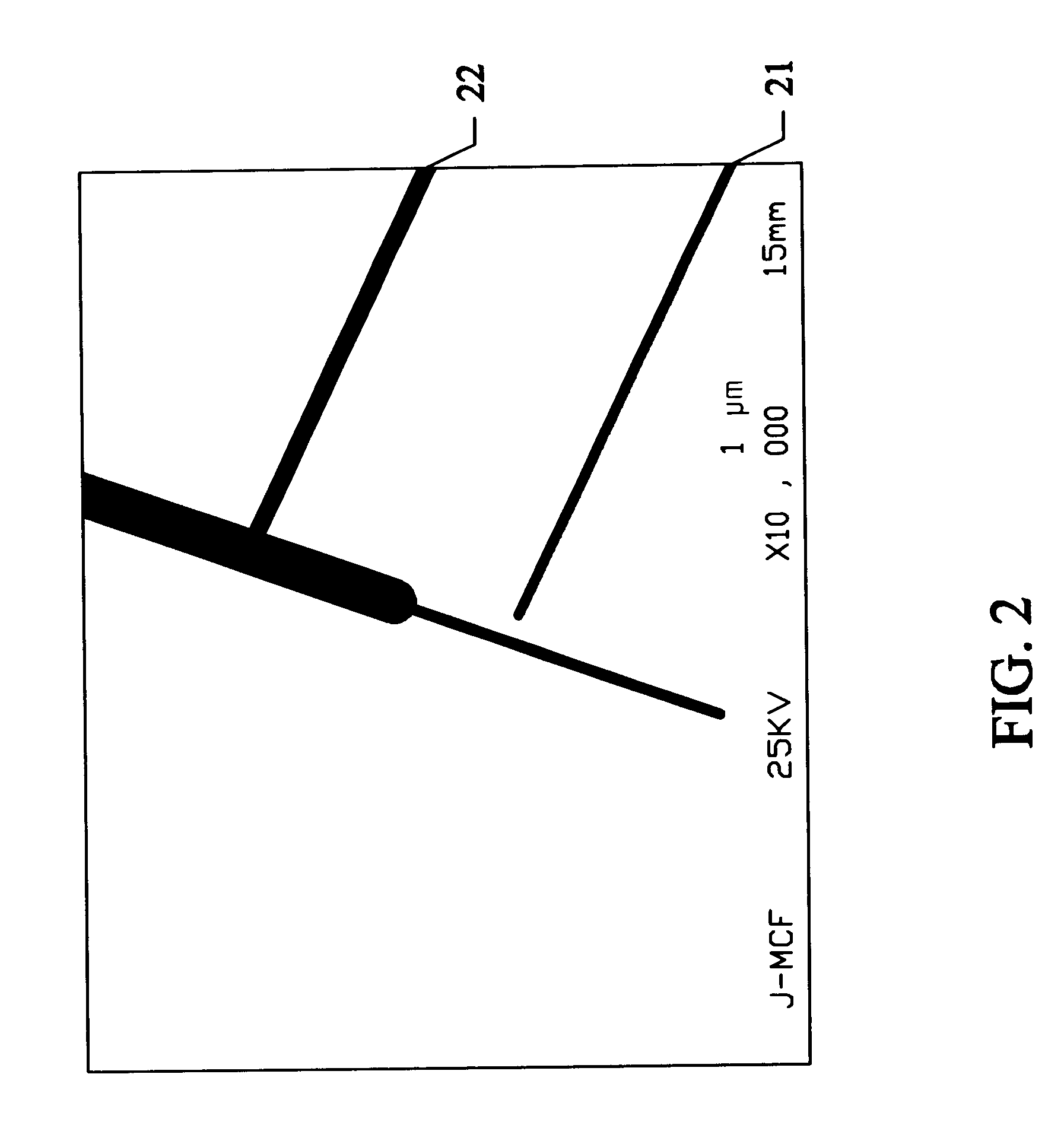
The preferred embodiment for the production of carbon nanotubes in the present invention results in nanotubes having a diameter between about 1 nanometer (nm) and about 100 nm with an integrally attached outer layer of graphitic material approximately 1 micrometer (.mu.m) to approximately 10 .mu.m in diameter. The much larger diameter of the graphitic outer layer becomes a handle so that the nanotube probe can be manipulated under a conventional optical microscope. The handle also provides a means for attachment and greatly enhances the utility of carbon nanotubes in a variety of scanning probe microscopes, electron microscopes and on a substrate as an electron emitter for flat panel displays.

Problems solved by technology

Together, the smallness of the nanotubes and the chemical properties of carbon atoms packed along their walls in a honeycomb pattern are responsible for their fascinating and useful qualities and, present significant production challenges.
The references reveal that prior art methods for producing carbon nanotubes give undesirably low yields.
However, the silicon nitride pyramid-tip scanning probe microscope can not meet the requirements of the semiconductor industry where a deep narrow trench of approximately 200 nm width and 500 nm depth is to be scanned.

Method used


Image

  • Carbon nanotube with a graphitic outer layer: process and application
  • Carbon nanotube with a graphitic outer layer: process and application
  • Carbon nanotube with a graphitic outer layer: process and application

Examples


Embodiment Construction

milligrams (mg) of FeNi nanoparticles, comprising a 1:1 ratio of Fe and Ni, are deposited on a silicon substrate having a surface area of approximately 300 cm.sup.2 in 50-100 Torr argon atmosphere. The FeNi transition metal catalyst on silicon substrate is removed from the evaporator and placed in a thermal catalytic vapor deposition (CVD) system consisting of a quartz tube inserted into a furnace.

The reactor vessel is heated to approximately 725.degree. C. with a flow of 50% argon and 50% hydrogen for 30 to 60 minutes. This purges the vessel of undesirable impurities and reduces oxides. Next, a gas flow comprising 10% methane (CH.sub.4) and 90% argon (Ar), is introduced to the reactor at a temperature between approximately 725.degree. C. and 900.degree. C. for a period of thirty minutes to forty-five minutes for nanotube growth. Then the gaseous mixture being fed to the reactor vessel is changed to 5% methane, 5% hydrogen (H.sub.2) and 90% argon while the reactor is heated to tempe...


PUM

PropertyMeasurementUnit
Temperatureaaaaaaaaaa
Fractionaaaaaaaaaa

Abstract

A method for manufacturing carbon nanotubes with an integrally attached outer graphitic layer is disclosed. The graphitic layer improves the ability to handle and manipulate the nanometer size nanotube device in various applications, such as a probe tip in scanning probe microscopes and optical microscopes, or as an electron emitting device. A thermal chemical vapor deposition reactor is the preferred reaction vessel in which a transition metal catalyst with an inert gas, hydrogen gas and a carbon-containing gas mixture are heated at various temperatures in a range between 500° C. and 1000° C. with gases and temperatures being adjusted periodically during the reaction times required to grow the nanotube core and subsequently grow the desired outer graphitic layer.

Description

The present invention relates to a novel method of manufacturing carbon nanotubes, and in particular to the production of a structure comprising a carbon nanotube with an outer graphitic layer that can function as a handle for attaching and / or manipulating the tip of the nanotube.BACKGROUND AND PRIOR ARTMaterial scientists have been exploring the properties of fullerenes which are geometric structures built of carbon atoms. In 1991, a new fullerene joined the buckyball, a cage-like structure built of 60 carbon atoms. Scientists found that the buckyball structure can be extended to form long slender tubes--carbon nanotubes--single molecules comprised of rolled graphene (graphite-like) sheets capped at each end. Thus, carbon nanotubes, the newest fullerene structure, are effectively buckyballs played out as long strands, so thin they can not be seen under an ordinary microscope and certainly not with the naked eye. In fact, it is suggested by Boris I. Yakobson and Richard E. Smalley i...

Claims


Application Information

Patent Timeline
IPC IPC(8): C01B31/00C01B31/02
CPCB82Y30/00B82Y40/00C01B31/0233D01F9/127D01F9/1271D01F9/1272D01F9/133Y10T428/2918Y10S977/742Y10S977/847Y10S977/86Y10S977/869Y10S977/745Y10T428/2991C01B32/162
Inventor CHOW, LEEZHOU, DANKLECKLEY, STEPHEN
Owner CENT FLORIDA UNIV OF
Learn More