Low voltage differential logic

a low voltage differential logic and logic technology, applied in logic circuit coupling/interface arrangement, instruments, pulse techniques, etc., can solve the problems of unnecessary power consumption, the power consumption of those circuits to become an increasingly critical factor

Inactive Publication Date: 2002-04-16
ORACLE INT CORP
View PDF2 Cites 11 Cited by
  • Summary
  • Abstract
  • Description
  • Claims
  • Application Information

AI Technical Summary

Problems solved by technology

Increasing demands for smaller, better, and faster electronic circuits having increasingly greater levels of functionality in a smaller package have caused the power consumption of those circuits to become an increasingly critical factor in circuit design.
While prior art circuits such as that seen in FIG. 1 are useful for their intended purpose, the supply voltages required to operate the circuit are higher than necessary and therefore cause unnecessary power consumption.

Method used


Image

  • Low voltage differential logic
  • Low voltage differential logic
  • Low voltage differential logic

Examples


Embodiment Construction

Those of ordinary skill in the art will realize that the following description of the present invention is illustrative only and not in any way limiting. Other embodiments of the invention will readily suggest themselves to such skilled persons who are familiar with this disclosure.

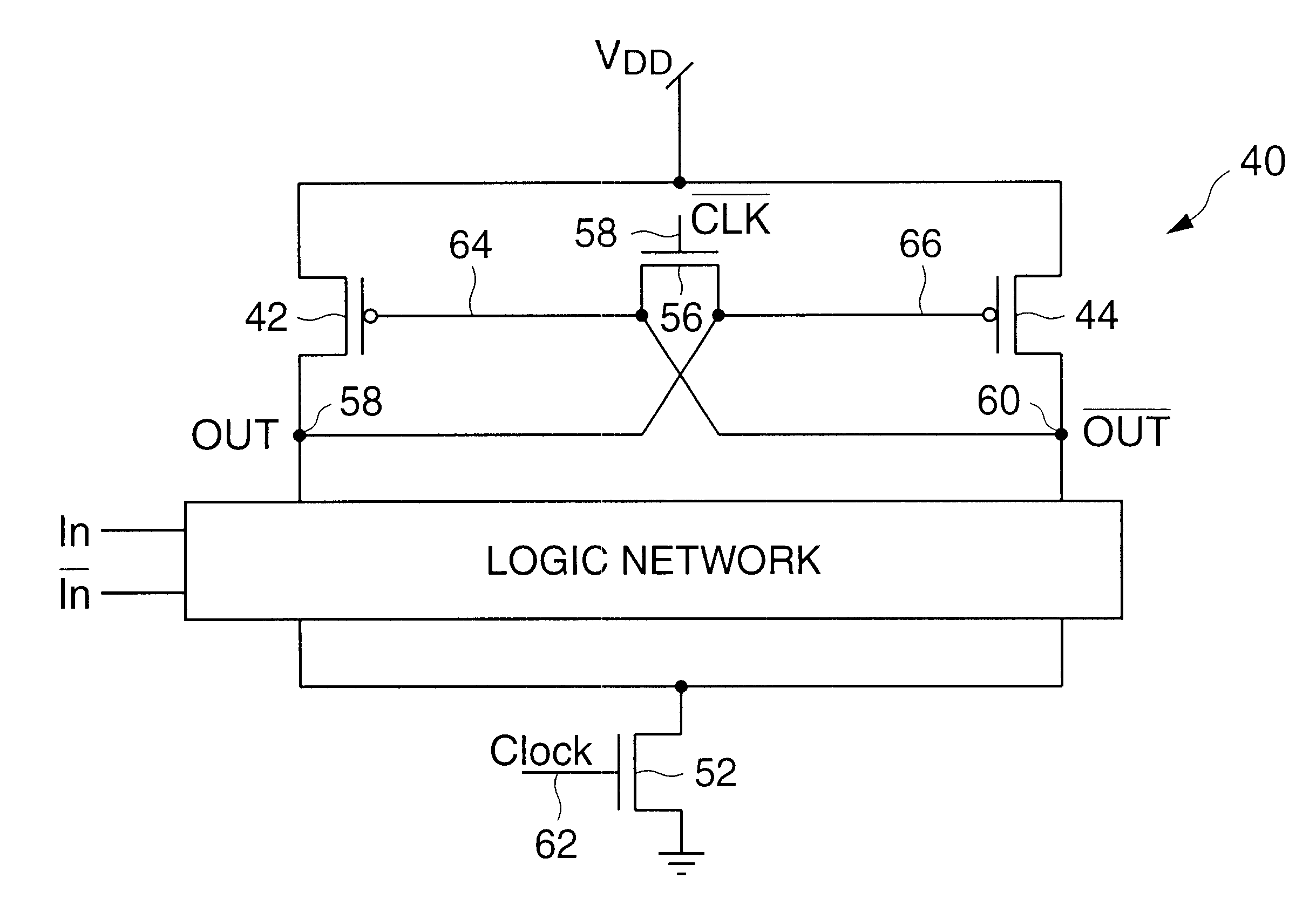
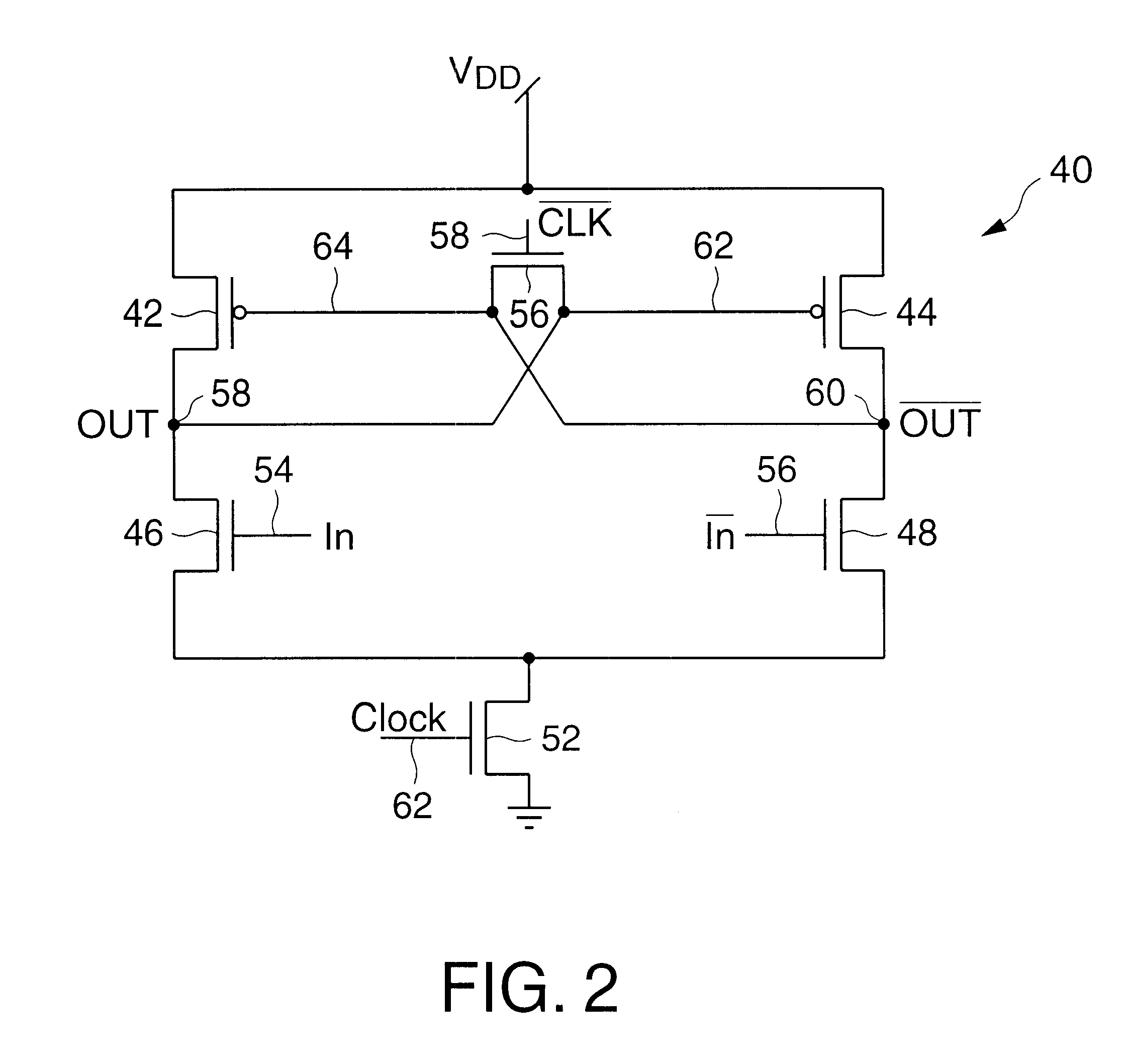
The present invention provides a high-speed CMOS circuit for performing logical functions but which consumes significantly less power than prior art circuits. It operates in two phases, precharge and evaluate. The precharge phase is when the clock signal inputs are at a logical low. The evaluate phase is when the clock signal inputs are at a logical high.

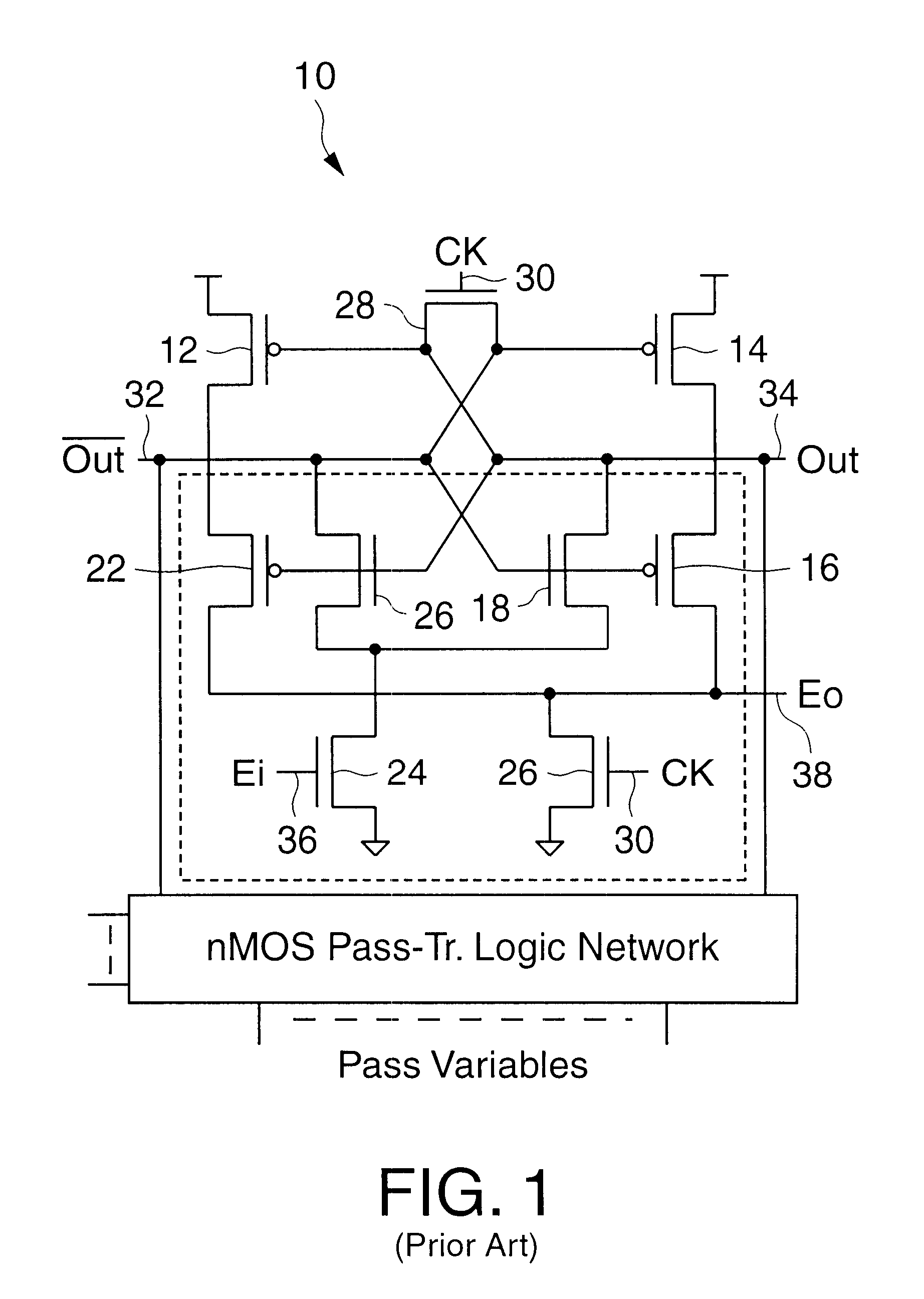
The supply voltage for prior art circuits is typically four to five times the threshold voltage of included transistors. However, the supply voltage for one embodiment of the present invention is approximately 1.0 VDC, or approximately 2.5 times the threshold voltage. By using a much smaller supply voltage, present invention circuits consume significantly...


PUM


Abstract

A low voltage differential circuit is described herein including a complementary logic tree having first, second and third inputs and two outputs, the logic tree for performing a desired logical function on signals received the the first input, thereby opening a pathway for current flow between at least one of the following: the second input and the first output, the second input and the second output, the third input and the first output, the third input and the second output. The circuit further includes a first transistor having a first gate, a first source, and a first drain, the first drain connected to the first output, the first source being connected to a supply voltage, a second transistor having a second gate, a second source, and a second drain, the second source connected to the first gate, the second drain connected to the first drain; and a third transistor having a third gate, a third source, and a third drain, the third source being connected to a supply voltage, the third gate being connected to the second drain, the third drain connected to the second source and the second output.

Description

1. Field of the InventionThe present invention relates to high-speed electronic circuits. More particularly, the present invention provides a low-power, high speed VLSI apparatus using voltage scaling.2. The Background ArtIncreasing demands for smaller, better, and faster electronic circuits having increasingly greater levels of functionality in a smaller package have caused the power consumption of those circuits to become an increasingly critical factor in circuit design.In most integrated circuits, it is considered beneficial to minimize the power consumption of individual circuits making up a system. Prior art VLSI systems use charge recycling differential logic (CRDL) circuits to transmit information from one location in an integrated circuit to another. One example of such a CRDL circuit is shown in FIG. 1.Referring to FIG. 1, CRDL circuit 10 includes transistors 12, 14, 16, 18, 20, 22, 24, 26 and 28. As with other dynamic circuits, circuit 10 operates in two phases, a prechar...

Claims


Application Information

Patent Timeline
Patent Type & Authority Patents(United States)
IPC IPC(8): H03K19/173
CPCH03K19/1738
Inventor CHOE, SWEE YEW
Owner ORACLE INT CORP
Why Eureka
Try Eureka