Analog to digital converter
a technology converter, applied in the field of analog to digital converter, can solve problems such as unstable output of a/d converter
- Summary
- Abstract
- Description
- Claims
- Application Information
AI Technical Summary
Benefits of technology
Problems solved by technology
Method used
Image
Examples
first embodiment
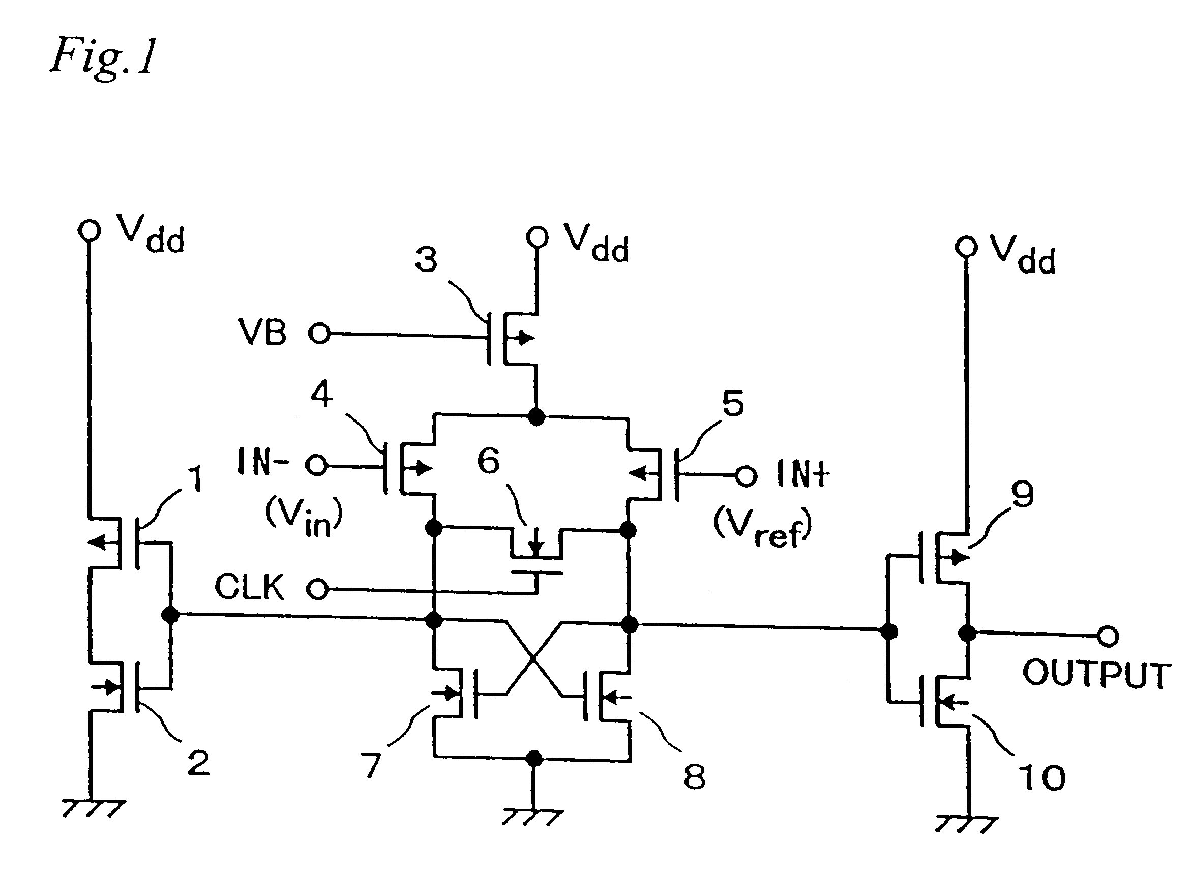
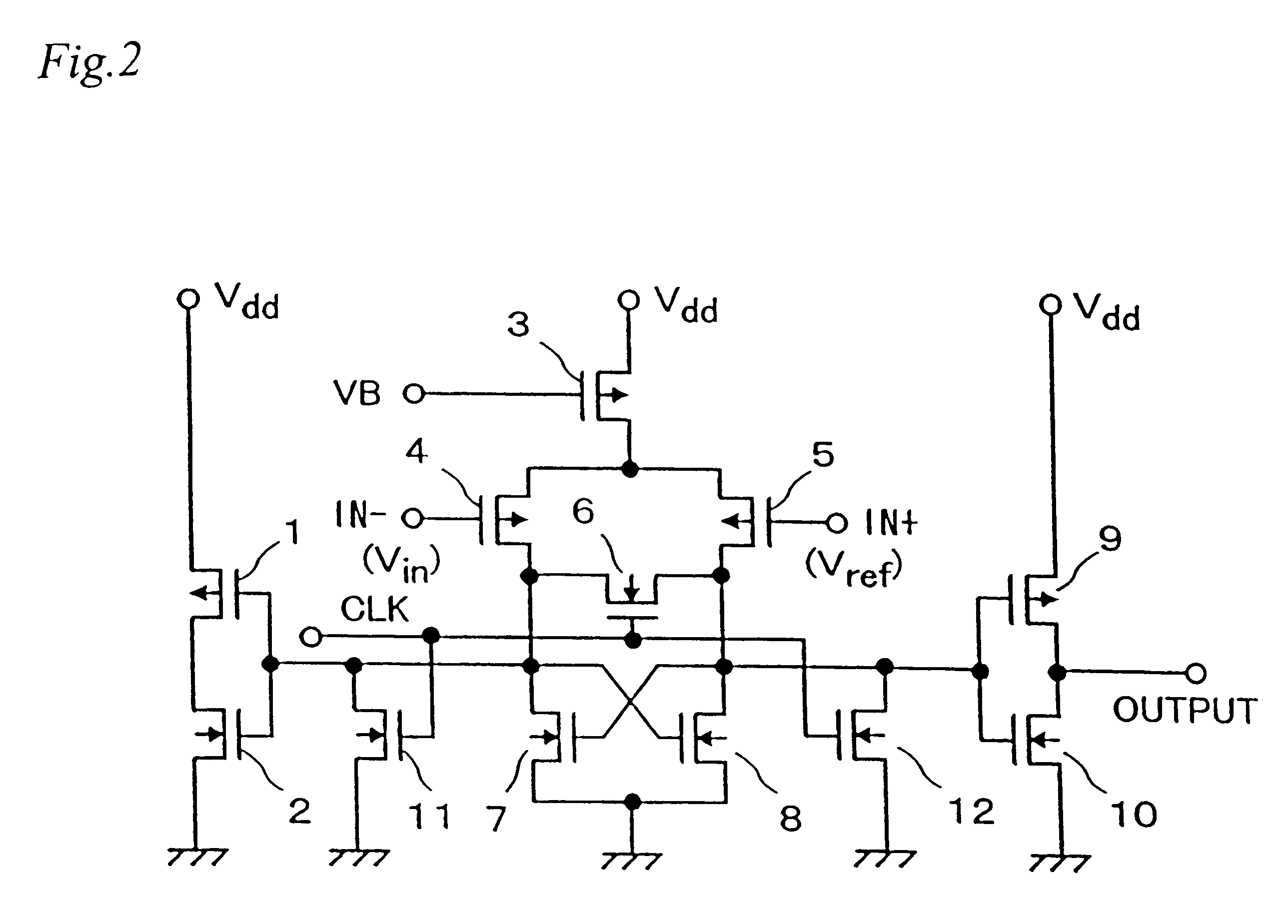
FIG. 1 is a circuit diagram showing a comparison circuit used in an A / D converter according to the present invention. In FIGS. 1, 1, 3, 4, 5, 9 are PMOSFETs and 2, 6, 7, 8, 10 are NMOSFETs.
In a central portion, a supply voltage Vdd is commonly input through the PMOSFET 3 to source terminals of the PMOSFETs 4 and 5. Drains terminals of the PMOSFETs 4 and 5 are connected to drain terminals of the NMOSFETs 7 and 8. Source terminals of the NMOSFETs 7 and 6 are commonly to a ground. A gate terminal of the NMOSFET 7 is connected to the drain terminal of the NMOSFET 8, and a gate terminal of the NMOSFET 8 is connected to the drain terminal of NMOSFET 8, thus crossing connection is provided. The NMOSFET 6 is connected between the drain terminals of the PMOSFETs 4 and 5. A comparison clock is input to a gate terminal of the NMOSFET 6. The drain terminal of the PMOSFET 4 is connected to a gate terminal of a CMOS inverter consisting of the PMOSFET 1 and NMOSFET 2 at a left side. The drain term...
second embodiment
FIG. 5 is a block diagram showing the A / D converter according to the present invention. In FIG. 5, 31 to 33, 41, 50 and 69 are multiplexers, 34 to 36, 42 to 45, 51 to 55 and 61 to 66 are input capacitances, 37, 46, 56 and 67 are switches, 38, 47, 57 and 68 are threshold setting circuits, 39, 48, 58 and 69 are comparison circuits, and 40, 49, 59 and 69 are inverters.
This A / D converter is a voltage driven type similar to the circuits in Japanese Patent Publication Hei09-083364, and additionally includes means for setting from outside an upper and lower limits of A / D conversion such that the input voltage between the upper and lower limits is converted into a digital data and a high resolution is obtained.
In this embodiment, the comparison circuits 39,48, 58 and 69 are non-inverted comparison circuits based on the comparison circuits in FIGS. 1 and 2. The conversion performance is similar to that in the first embodiment in FIGS. 3 and 4. At the leading edge of the comparison clocks CLK...
third embodiment
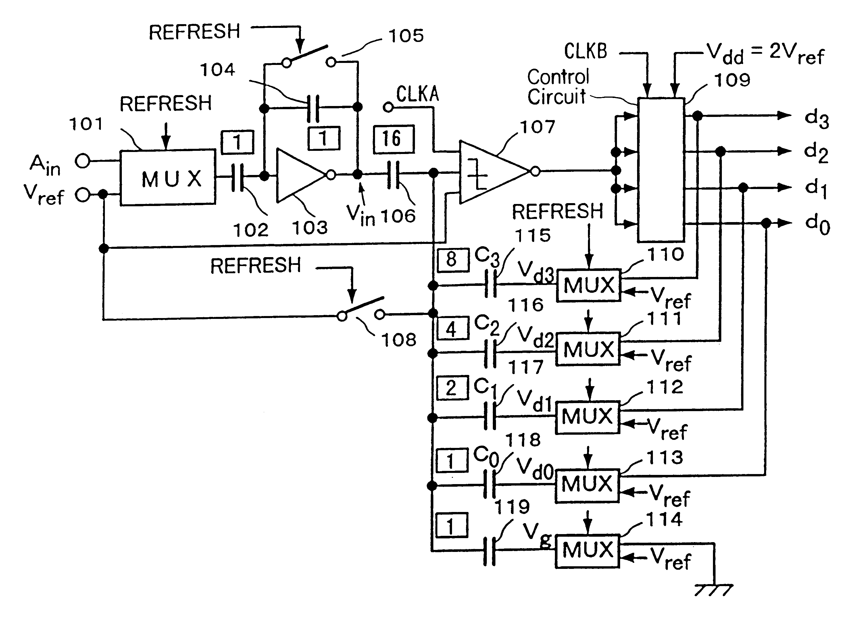
FIG. 7 is a block diagram showing the A / D converter according to the present invention. In FIG. 7, 101 is a multiplexer, C102 is an input capacitance, 103 is an inverting amplifier, C104 is a feedback capacitance, 105 is a switch, C106 is an input capacitance, 107 is a comparison circuit, 108 is a switch, 109 is a control circuit, 110 to 114 are multiplexers, C115 to C118 are capacitances for controlling thresholds, and C119 is a capacitance for adjusting threshold.
This embodiment is a sequential type A / D converter for converting an analog input voltage Ain into a (m+1) bit digital data of dm to d0, and m+1=4. Since analog input voltage Ain must be kept constant during one time A / D conversion, it is necessary that the analog input voltage Ain itself has a little drift, or that the analog input voltage Ain is once held by a sampling and holding circuits. The analog input voltage Ain is inverted by the inverting amplifier 103 with basis of the reference voltage Vref and input to the c...
PUM
 Abstract
Description
Claims
Application Information
 - R&D
- Intellectual Property
- Life Sciences
- Materials
- Tech Scout
- Unparalleled Data Quality
- Higher Quality Content
- 60% Fewer Hallucinations
Browse by: Latest US Patents, China's latest patents, Technical Efficacy Thesaurus, Application Domain, Technology Topic, Popular Technical Reports.
© 2025 PatSnap. All rights reserved.Legal|Privacy policy|Modern Slavery Act Transparency Statement|Sitemap|About US| Contact US: help@patsnap.com


