IC module, method of manufacturing the same and IC card provided with IC module

Inactive Publication Date: 2001-10-30
ROHM CO LTD
View PDF18 Cites 51 Cited by
  • Summary
  • Abstract
  • Description
  • Claims
  • Application Information

AI Technical Summary

Benefits of technology

The present invention is intended to eliminate the conventional problems described above and its object is to provide a technique capable of providing good protection of an IC chip and an antenna coil.
In the manufacturing method, a flattened coil, that is, a coil having a small thickness is used. When a melted resin is introduced into the cavity while the coil is housed, flow of the melted resin from the periphery of the cavity to the center is hardly hindered by the coil, and the melted resin can flow smoothly in the cavity.
Especially when such a coil is adopted that is formed to a tapered shape so that the cross section of the perimeter portion decreases in thickness toward the perimeter, the melted resin can flow more smoothly, and the melted resin can be distributed to the portions over and under the coil and spread in the entire cavity. It can prevent formation of a void and a pinhole in the resin package at the end of designing. Since the flow of the melted resin is distributed to the portions over and under the coil, the coil will not excessively be lifted upward. Further, since the resin can be set while it sufficiently flows to an upper portion of the coil, the coil can not be exposed from the surface of the resin package or it can not easily be exposed at the end of designing.
Further, a spacer that is formed of a material having the same or similar physical properties to those of the packaging resin can be adopted. In this case, the spacer and the resin package match well, preventing, for example, stripping of the resin package around the spacer after molding.
Since the IC cards in the seventh and eighth aspects above include the IC module in the first or third aspect above, they can of course have the effects of the IC module in the first or third aspect. When the cover sheet is stuck on the surface of the card body, the IC card, especially the IC module can be protected effectively.

Problems solved by technology

Then, it can not be expected but that the force caused by a user's handling or the force received from the transportation system of a mechanical card reader causes such thin cards to bend to some extent.
A problem in this case is influences on a built-in IC chip when the IC card bends.
In this case, the IC chip may be stripped out of a prescribed interconnection pattern or the IC chip itself may be damaged.
In other words, a power supply path to the IC chip may be cut stopping supply of power, the contents stored in the IC chip may be lost, and so on.
However, the following disadvantages have been caused in the resin packaging process.
Firstly, when a coil is used as an antenna coil and a substrate 2 on which an IC chip 3 is placed is packaged together with the coil with a resin, disadvantages have been caused as described below.
When the resin sets while coil 20A is lifted upward, coil 20A may be exposed from the surface of the resin package or it may easily be exposed, and therefore coil 20A is easily damaged.
If the melted resin sets in this situation, IC chip 3 may be exposed from the surface of the resin package or it may easily be exposed.
Thus, IC chip 3 is susceptible to damages.

Method used


Image

  • IC module, method of manufacturing the same and IC card provided with IC module
  • IC module, method of manufacturing the same and IC card provided with IC module
  • IC module, method of manufacturing the same and IC card provided with IC module

Examples


Embodiment Construction

The preferred embodiments of the present invention will be described below in detail with reference to the drawings.

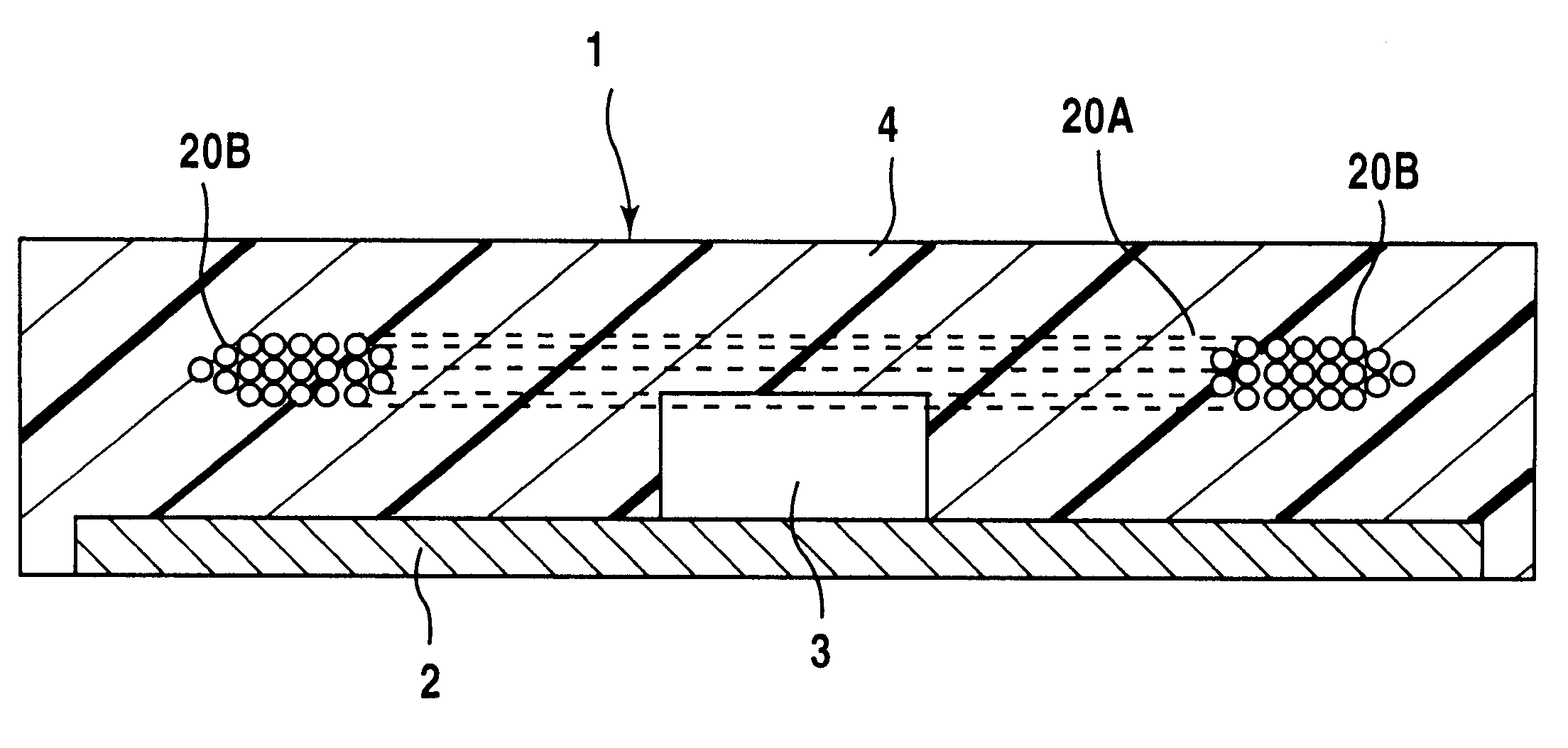
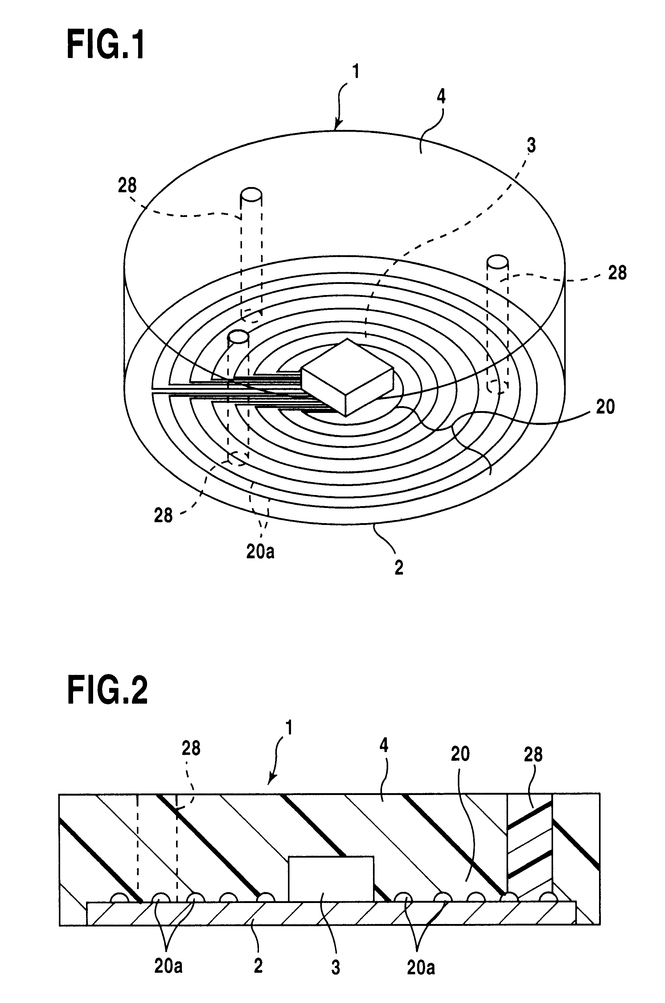
As shown in FIGS. 1 and 2, an IC module 1 includes a circular substrate 2, an IC chip 3 placed on substrate 2, an antenna coil 20 formed on the surface of substrate 2, and a resin package 4 covering substrate 2 and IC chip 3, and the IC module is formed to a column shape as a whole.

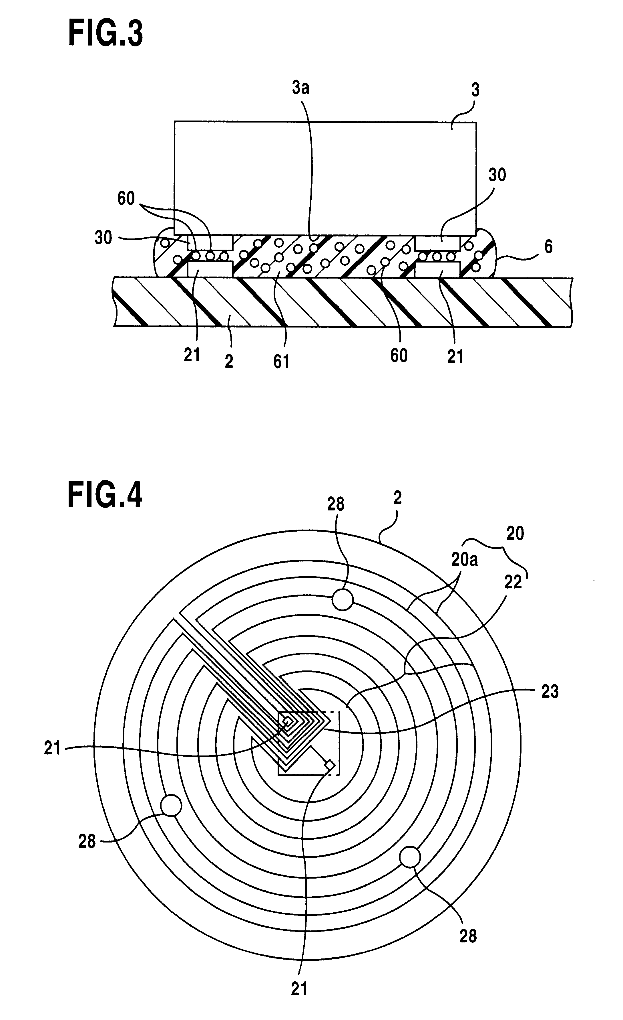
IC chip 3 has EEPROM memories, for example, and other condensers that are integrally formed, and the chip is formed to a rectangular parallelepiped shape as a whole as can be seen in FIG. 1. Here, IC chip 3 is mainly used as a memory having an information storage function. As shown in FIG. 3, antenna-connected electrodes 20, are formed on the main surface 3a of IC chip 3, and electrodes 30, are formed to protrude from main surface 3a by plating electrode pads knot shown) with gold.

As shown in FIG. 4, substrate 2 is formed to a circular shape by using a resin such as a polyimide film that has...


PUM

PropertyMeasurementUnit
Currentaaaaaaaaaa
Thicknessaaaaaaaaaa
Heightaaaaaaaaaa

Abstract

In the method of manufacturing an IC module (1) including a resin packaging process using upper and lower dies (5) for forming a cavity (50) while the dies are clamped, the resin packaging process is carried out by introducing a melted resin while a substrate (2) on which an IC chip (3) is placed and a coil (20A) which has a doughnut shape when observed from above and is flattened as a whole are housed in the cavity (50). When a substrate (2) on which an antenna coil (20) is patterned is to be packaged with a resin, the resin packaging process is carried out by forming a spacer (28) having an equal and almost equal height to the height of the cavity (50) on the substrate (2), housing it in the cavity (50), and introducing a melted resin. Instead of forming the spacer (28) on the substrate (2), a substrate (2) housed in a cavity (50) may be sucked. The manufacturing method can provide good protection of an IC chip and an antenna coil.

Description

The present invention relates to an IC card, such as an "ID card," provided with an information storage function by containing an IC chip, an IC card module incorporated in the IC card and including an IC chip, and a method of manufacturing the module.As is well known, there are cards with an information storage function. Some of them store information by magnetic stripes and others are "IC cards" including IC memories.Advantageously, such cards are suitably firmed as "non-contact type information storage cards" and, when compared with magnetic stripe type cards, they can easily be increased in information storage capacity and are highly effective in preventing forgery. It is therefore expected to achieve IC cards having a higher information processing or communication function by incorporating memory chips, CPUs and the like with increased storage capacity into the cards. In the future, it is expected that the IC cards be utilized as telephone cards or tools for carrying informatio...

Claims


Application Information

Patent Timeline
IPC IPC(8): B29C45/14G06K19/077B29C45/00B42D15/10G06K19/07H01Q7/00
CPCB29C45/14647G06K19/07724G06K19/07745G06K19/07747G06K19/07749B29C45/0046B29L2031/3456H01L2224/16H01L2924/01057H01L2924/01078H01L2924/01079G06K19/067
Inventor HIRAI, MINORUUEDA, SHIGEYUKIMIYATA, OSAMUHORIO, TOMOHARU
Owner ROHM CO LTD
Why Eureka
Try Eureka