
Method for simultaneously forming a storage-capacitor electrode and interconnect

a technology of storage capacitor and electrode, which is applied in the field of semiconductor memories, can solve the problems of reducing the operational efficiency of dram noise, reducing the operational efficiency of dram, and causing the amplifier of dram to output erroneous logic values,

Inactive Publication Date: 2000-09-26
GLOBALFOUNDRIES INC
View PDF29 Cites 45 Cited by
  • Summary
  • Abstract
  • Description
  • Claims
  • Application Information

AI Technical Summary

Benefits of technology

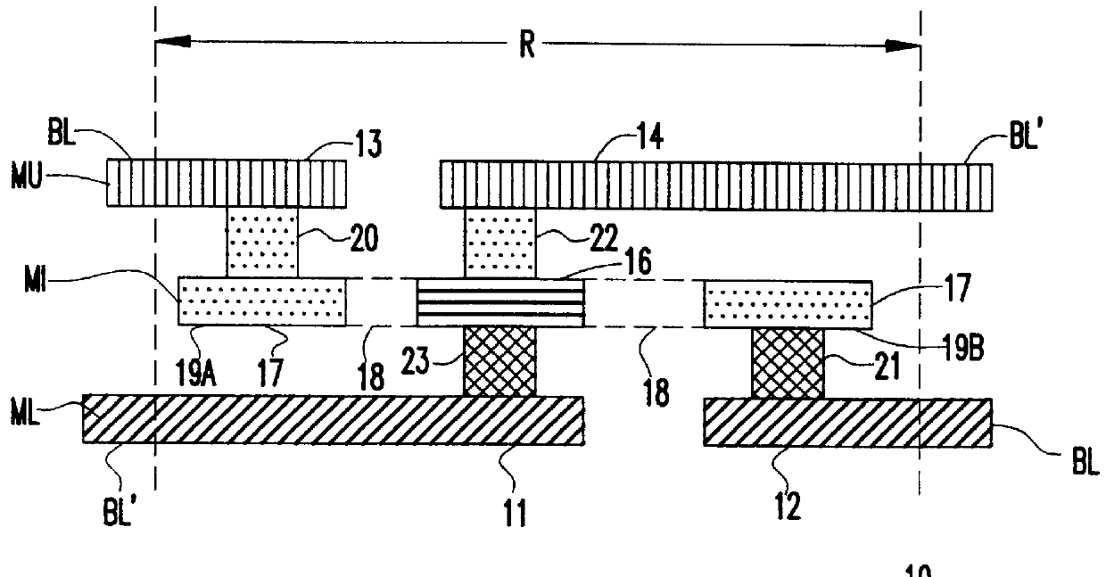
It is another objective of the present invention to provide a DRAM memory cell of the aforementioned type, wherein the storage-capacitor level of the memory cell is located between chip interconnects and / or complementary bit lines of the DRAM, thereby increasing integration density compared with conventional DRAMs which use special, dedicated wiring levels to make these interconnections.
It is another objective of the present invention to provide a method for making a DRAM memory cell of the aforementioned type, wherein the capacitor electrode is formed simultaneously with an electrode of at least one of the storage capacitors of the cell, thereby reducing the number of steps and the cost required to make the DRAM.

Problems solved by technology

They also provide extremely rapid access, but at the cost of substantial power consumption, expense, and wafer space.
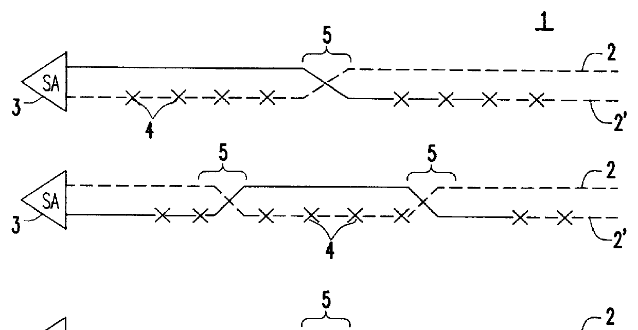
One effect which reduces the operational efficiency of a DRAM is noise which is capacitively coupled between adjacent bit lines.
This noise, among other things, causes the sense amplifiers of the DRAM to output erroneous logic values.
Dedicated wiring layers are undesirable because they increase the cost and complexity of the fabrication process, as well as reduce integration density.
Moreover, the storage capacitors in these DRAMs are often formed in layers beneath the bit lines, which further reduces integration density.
The height of these capacitors, however, has proven troublesome because of the additional cost required in patterning their thick lower electrode, which further reduces integration density.
The Kagenishi approach, however, actually decreases integration density because any improvement realized from using a bit line as a capacitor electrode is offset by the presence of compensation capacitors in the first place.

Method used


Image

  • Method for simultaneously forming a storage-capacitor electrode and interconnect
  • Method for simultaneously forming a storage-capacitor electrode and interconnect
  • Method for simultaneously forming a storage-capacitor electrode and interconnect

Examples


first embodiment

the method of the present invention, thus, forms a DRAM memory cell having an intermediate wiring level between metal layers (69,63) and 100. This intermediate wiring level includes at least one wiring layer in the form of lower capacitor electrode 72 which electrically connects metal layers 63 and 100.

Metal layers 63 and 100 may be one of a variety chip features. For example, metal layers 63 and 100 may be portions of a bit line disposed on different levels of the DRAM structure. Under these circumstances, electrode 95 may advantageously be used to establish a flipped connection between these bit lines portions. Alternatively, metal layers 63 and 100 may be interconnects attached to one or more support circuits of the DRAM, which are then connected by electrode 72 through studs 97 and 64. Still further, electrode 72 may be used to connect support circuits to a diffusion region or gate electrodes in substrate 52 via elements 64, 63, and 62 where support device 54 may eventually rece...

second embodiment

the present invention, thus, forms a DRAM memory cell structure having an intermediate wiring level between metal layers 63 and 100. This intermediate wiring level is in the form of a layered structure which includes lower capacitor electrode 72, dielectric 72, and upper capacitor electrode 120. In this embodiment, only lower capacitor electrode 95 is used to electrically connect metal layers 63 and 100, which may be bit-lines, support circuits interconnects, or any of the other types of interconnects and global wirings previously discussed. For example, the layered structure of the second embodiment especially well suited for use as either capacitor electrode 16 or 17 forming the flipped bit-line connections shown in FIGS. 2 and 3.

While the upper capacitor electrode 120 is not used as an interconnect in the second embodiment, it nevertheless is beneficial in a number of respects. For example, the upper capacitor electrode advantageously improves the planarity of the overlying diele...

third embodiment

the present invention, thus, forms a DRAM memory cell structure having an intermediate wiring level connecting metal layers 100 and 200. This intermediate wiring layer is in the form of a layered structure which includes lower capacitor electrode 95, dielectric 75, and upper capacitor electrode 120. In this embodiment, only upper electrode 120 is used to electrically connect metal layers 100 and 200, which may be support circuits interconnects or any of the other types of global wiring previously discussed.

For all embodiments herein, the upper capacitor electrode may be made from platinum (Pt) and the dielectric from (Ba,Sr)TiO.sub.3. In selecting these materials, it is noted that there are usually more constraints placed on the choice of materials for the lower electrode than on the upper electrode, for example, because the lower electrode must be able to withstand high temperature annealing. A refractory metal (e.g., one having a high melting point), therefore, is usually selected...


PUM


Abstract

A DRAM memory cell array includes a wiring layer formed at a storage-capacitor level of the cell for establishing a flipped connection of complementary bit lines, or for connecting support circuits in a DRAM cell array. The wiring layer includes a lower capacitor electrode and upper capacitor electrode which are formed simultaneously with respective plates of a storage capacitor. Both capacitor electrodes may be used to form distinct interconnections within a DRAM cell array.

Description

1. Field of the InventionThe present invention generally relates to semiconductor memories, and more particularly to structures and methods for forming interconnections within a semiconductor memory.2. Description of the Prior ArtGenerally speaking, there are two types of semiconductor memories. In the first type, data stored in the individual cell locations of the memory cannot be altered. Consequently, these memories are referred to as read-only memories. In the second type, data stored in each cell location can be altered, i.e., are subject to both read and write operations. The latter memories have therefore been called random-access memories.Random-access memories (RAMS) come in various forms. Static random-access memories (SRAMs) , for example, store data as long as they are connected to a power source. They also provide extremely rapid access, but at the cost of substantial power consumption, expense, and wafer space. Dynamic random access memories (DRAMs)use capacitive stora...

Claims


Application Information

Patent Timeline
Patent Type & Authority Patents(United States)
IPC IPC(8): H01L21/70H01L23/522H01L23/52H01L21/8242H01L21/02H10B12/00
CPCH01L23/522H01L27/10885H01L27/10894H01L28/55H01L2924/0002H01L2924/00H10B12/09H10B12/482
Inventor GAMBINO, JEFFREY P.BRONNER, GARY B.KOTECKI, DAVID E.RADENS, CARL J.
Owner GLOBALFOUNDRIES INC
Learn More