
Self-initiated self-refresh mode for memory modules

Inactive Publication Date: 2000-09-12
MARVELL ASIA PTE LTD
View PDF13 Cites 70 Cited by
  • Summary
  • Abstract
  • Description
  • Claims
  • Application Information

AI Technical Summary

Problems solved by technology

However, this technique requires that all of the banks of memory be inoperative during the clock time during which self-refresh is being entered, which time can be as long as several hundred microseconds.

Method used


Image

  • Self-initiated self-refresh mode for memory modules
  • Self-initiated self-refresh mode for memory modules
  • Self-initiated self-refresh mode for memory modules

Examples


Embodiment Construction

)

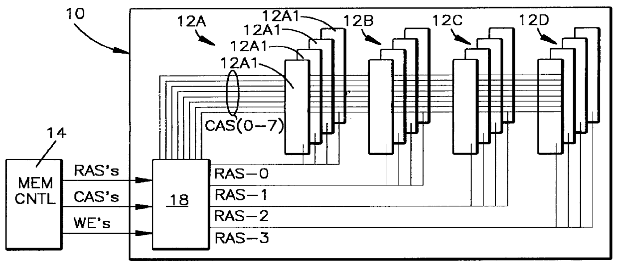
Referring now to the drawings and to the present FIG. 1, an asynchronous DRAM card is shown somewhat diagrammatically and designated by the reference character 10. Conventionally, in certain configurations, a DRAM card has a plurality of banks of DRAM (Dynamic Random Access Memory) chips, four of which banks are shown and designated as 12a, 12b, 12c and 12d. Each bank 12a, 12b, 12c, and 12d is made up of a number of DRAM chips, the number of chips being dependent upon the bus size and the type of chip. For illustration purposes, but not by way of limitation, each bank is shown with four chips, 12a1, 12a2, 12a3, and 12a4; 12b1, 12b2, 12b3, and 12b4; 12c1, 12c2, 12c3, and 12c4; and 12d1, 12d2, 12d3, and 12d4. This represents a chip configuration in each bank of four x16 DRAM chips. Other possible arrangements of chip configurations include two x32 DRAM chips or eight x8 DRAM chips or 16.times.4 DRAM chips. These are typical configurations for 64 bit wide data busses.

The DRAM card 10 ...


PUM


Abstract

A method and apparatus for selectively causing each bank of a number of banks of DRAMs of a DRAM memory card to enter into the self-refresh mode without affecting the operation of any other bank. In the computer system incorporating the SIMM or DIMM type DRAM cards, each bank of memory on each card has a RAS signal specific to that specific bank. One or more CAS signals are supplied across all of the memory banks, on all cards. Thus, each memory bank is accessed separately for a read / write operation by the RAS becoming active before the CAS becomes active; and refresh takes place by the CAS signal becoming active before the RAS signal becomes active. The number of clock cycles or refresh cycles between active RAS signals to each memory bank are counted. If RAS does not become active for N clock or refresh cycles, a signal is provided within each respective memory bank and that memory bank will immediately, or preferably after M additional clock or refresh cycles enter self-refresh mode without affecting the operation of any other bank. At the same time, the memory controller counts cycles of RAS inactivity for each DRAM bank it controls. A signal is also provided to a register to require a double read / write on the next active read / write cycle to that bank, for reactivating that bank from the self-refresh mode when RAS signal specific to that bank becomes active while CAS is inactive.

Description

This invention relates generally to a technique for entering or leaving self-initiated self-refresh or "sleep" mode for memory modules, and more particularly to a method and structure for causing individual banks of chips in memory modules to enter the self-refresh mode based on predetermined intervals of non-use in read / write operations for that particular bank.BACKGROUND INFORMATIONAs the amount of computer memory available on personal computers, and especially portables or lap-top computers, increases, the amount of power required to maintain the memory in an active state increases. Hence, it has become conventional practice to reduce the power used by the chips in the various memory banks of SIMMs and DIMMs when they are not in use by having the chips, or banks of chips enter a self-refresh mode in which power requirements are substantially decreased. In fact, power savings can be realized if individual banks of memory on SIMM and DIMM cards wherein there is more than one bank o...

Claims


Application Information

Patent Timeline
Patent Type & Authority Patents(United States)
IPC IPC(8): G11C11/406
CPCG11C11/406
Inventor DELL, TIMOTHY J.HAZELZET, BRUCE G.KELLOGG, MARK W.
Owner MARVELL ASIA PTE LTD
Learn More