Planar trenches

a technology of planar trenches and trenches, applied in the direction of basic electric elements, electrical equipment, semiconductor/solid-state device manufacturing, etc., can solve the problems of ineffective later processing to remove undesirable conducting materials, high mechanical stresses, short circuits

Inactive Publication Date: 2000-05-16
INFINEON TECH AG
View PDF7 Cites 7 Cited by
  • Summary
  • Abstract
  • Description
  • Claims
  • Application Information

AI Technical Summary

Benefits of technology

is to provide a method for eliminating the problem of strings of surplus conducting material remaining in grooves along trench edges.
In accordance with the invention this object is accomplished by providing extra amounts of trench material along the edges of the trenches in order to prevent the occurrence of grooves along the trench edges. In the case of silicon-based processing this is done by depositing on to the trench filling material a layer of polysilicon, oxide, nitride or the like which is then etched back by an anisotropic etch i.e. an etching process which attacks the layer to be etched significantly faster in the vertical direction hand in the horizontal. This leaves extra material along the trench edges. This process can take place before or after the oxide layer is grown on the polysilicon in the trench. In the case of non-oxidisable material such as oxide or nitride the thickness of the extra material after etching should be approximately the same as the height of the downward vertical step. In the case of polysilicon, the thickness of the polysilicon deposited is preferably chosen such that when all of the extra polysilicon is oxidised during the subsequent oxidation the resulting oxide layer has approximately the same height as the step height. The extra material in the form of oxides nitride or polysilicon srings along the trench edges protect from oxidation the underlying silicon which otherwise would be oxidised and produce regions of high mechanical stress. In the absence of regions of high mechanical stress the subsequent wet etching proceeds more evenly and the production of unwanted grooves at the trench edges is avoided. By using the same type of material that is used to fill the trench as the extra material less mechanical stress is produced in the trench after oxidation.
The oxidation of the extra thickness of the polysilicon material near to the trench edges also provides a thicker oxide layer near to the trench walls. By choosing the correct dimensions for the extra polysilicon strings it is possible to produce oxides layers at the trench edges which are substantially the same thickness as the surrounding oxide layers and in this way achieve a more planar surface. By a suitable choice of deposition temperature it is possible to adjust the grain size of deposited silicon i.e. deposition at 580.degree. C. produces amorphous silicon while deposition at 600.degree. C. produces micro-crystalline silicon and deposition at 620.degree. C. gives polycrystalline silicon. Amorphous silicon oxidises more quickly than micro-crystalline silicon which oxidises more quickly than polycrystalline silicon. It is therefore possible to adjust the relative oxidation rates of the trench material and the extra material to form a desired trench cross-sectional profile by adjusting the deposition temperature of the extra material.
A trench formation formed in accordance with the invention has a number of advantages. An obvious advantage is that the surface over the trench no longer has a vertical step which reduces the risk of undesirable material being trapped in the trench and later causing problems. An other advantage is that a more even planar surface is achieved after the oxide or nitride has been deposited or after the polysilicon has been deposited and etched back in a method according to the invention. A further advantage is that the mechanical stresses in the trench are reduced.

Problems solved by technology

This produces high mechanical stresses in these regions.
During further processing it is possible that these grooves become filled with conducting material to such a depth that later processing to remove undesirable conducting material is ineffective and strings of surplus conducting material remain in the grooves.
These strings can cause problems such as short circuits particularly if the strings are so high that they contact conductors laid over the trench.

Method used


Image

  • Planar trenches
  • Planar trenches
  • Planar trenches

Examples


second embodiment

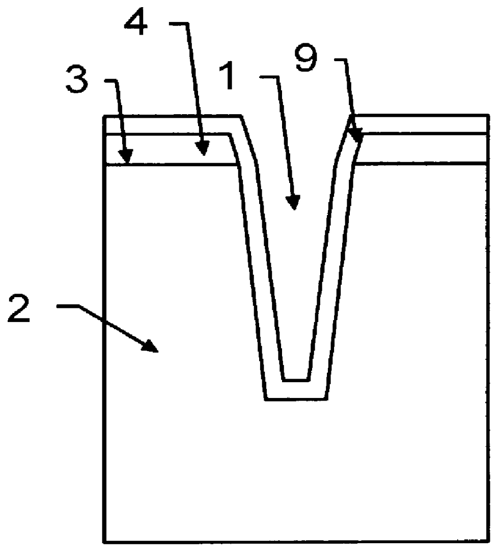
In a method according to the present trenches are formed using the processes described above with reference to FIGS. 2a-2d. The polysilicon 6 in the trench is then oxidised to form a layer of silicon oxide before the extra seams 20 of material are laid along the edges of the trenches. This layer of silicon oxide acts as a stop layer with respect to further processing and prevents the underlying polysilicon 6 in the trench from being etched or oxidised in the following processing stages. The polysilicon is preferably oxidised at a comparatively low temperature in the region of 800.degree. C. to 900.degree. C.

third embodiment

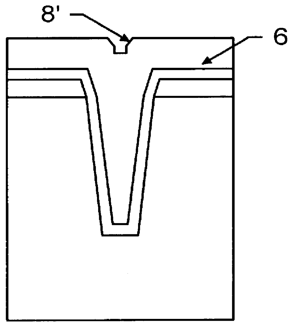
In the invention instead of polysilicon a further layer of oxide is deposited over the entire wafer, including the trench walls, after the steps of filling the trench with polysilicon and subsequent etching back of the polysilicon have been performed. The depth of this further layer is dependent on the height of the vertical step of the trench and the required height of the seams as described later. This oxide layer is then etched back to the earlier oxide layer with an anisotropic etch which etches primarily in the vertical direction thus leaving, as in the embodiment above, extra seams of material along the trench edges. The thickness of the extra seams (and thus the thickness of the deposited oxide layer) is chosen such that the remaining oxide layer along the trench edges has a thickness (height) substantially equal to that of the original insulating oxide layer and that the trench walls are displaced towards each other an amount sufficient to cover any regions of the trench edg...


PUM


Abstract

Method for improving the topography over trench structures in which the provision of extra poly-semiconductor material e.g. polysilicon or nitrate or oxide in the regions of the trench edges and, if necessary, the subsequent oxidation of the extra material prevents the occurrence of regions of high mechanical stress.

Description

The present invention relates to trenches in semiconductor products having a substantially planar surface.DESCRIPTION OF RELATED ARTIn order to isolate components in integrated circuits from each other refilled trench structures have been developed. There are many different methods of forming such trenches. The most common methods for making filled trenches are described in Wolf, S., "Silicon Processing for the VLSI Era Volume II", pages 45-56, ISBN-0-961672-4-5, 1990, Lattice Press USA. The main steps are that a trench is etched into the silicon substrate surrounding each component to be isolated on a wafer. An isolating oxide layer is then deposited in the trench and on the silicon substrate to isolate the component from the surroundings. The trench is then filled by depositing polysilicon over the whole wafer to a thickness which is sufficient to fill all the trench structures. Thus the polysilicon is also deposited on the oxide layer on the planar surfaces of the silicon substra...

Claims


Application Information

Patent Timeline
IPC IPC(8): H01L21/70H01L21/763H01L21/762
CPCH01L21/763H01L21/76202
Inventor SODERBARG, ANDERSOGREN, NILSSJODIN, H.ANG.KANZACKRISSON, MIKAEL
Owner INFINEON TECH AG
Why Eureka
Try Eureka