
Bipolar transistor with collector surge voltage protection

a bipolar transistor and collector technology, applied in the direction of diodes, semiconductor devices, semiconductor/solid-state device details, etc., can solve the problems of increasing the number of parasitic capacitors or inevitably forming, and so as to achieve the effect of not reducing the operation speed of the circuit including the transistor

Inactive Publication Date: 2000-01-11
LAPIS SEMICON CO LTD
View PDF8 Cites 10 Cited by
  • Summary
  • Abstract
  • Description
  • Claims
  • Application Information

AI Technical Summary

Benefits of technology

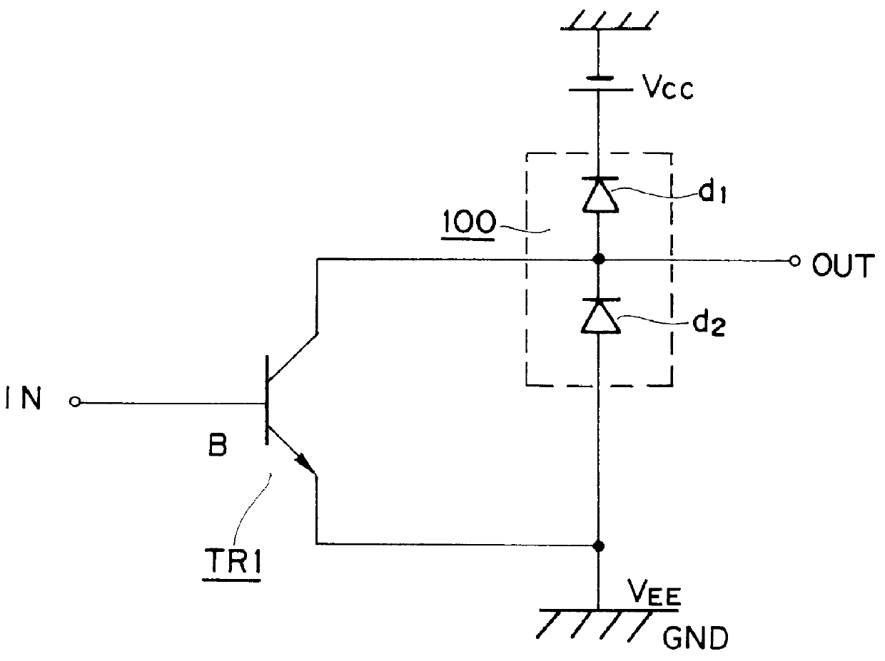
Accordingly, an object of this invention is to provide a semiconductor device provided with a planar bipolar transistor and a built-in ingredient acting as an element to protect the bipolar transistor from an external surge voltage e.g. an electrostatic surge voltage and the like, wherein the operation speed of a circuit including the transistor is not reduced by potential parasitic capacitors which otherwise accompany the built-in ingredients produced to protect the transistor from an external surge voltage e.g. an electrostatic surge voltage and the like.
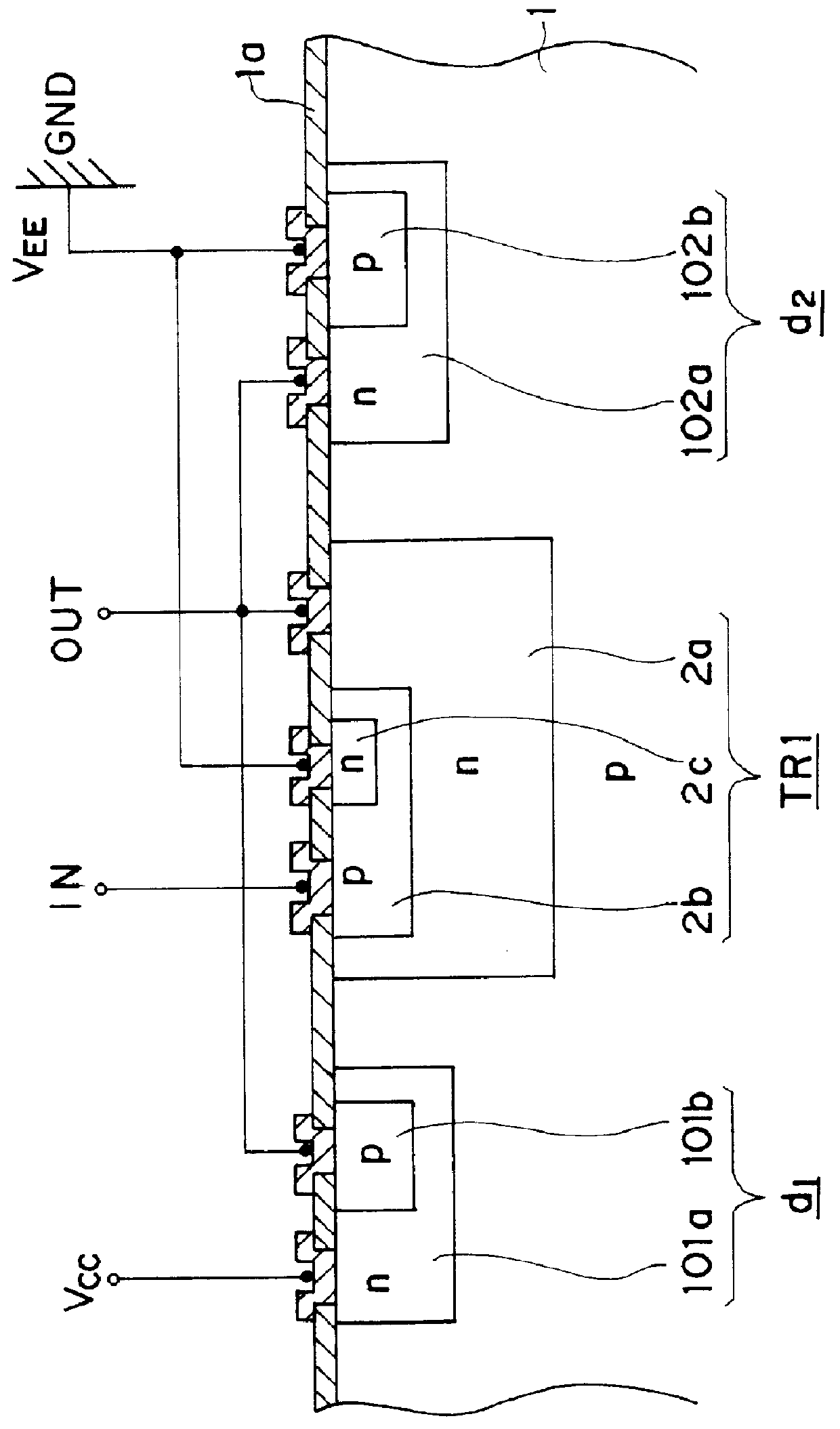
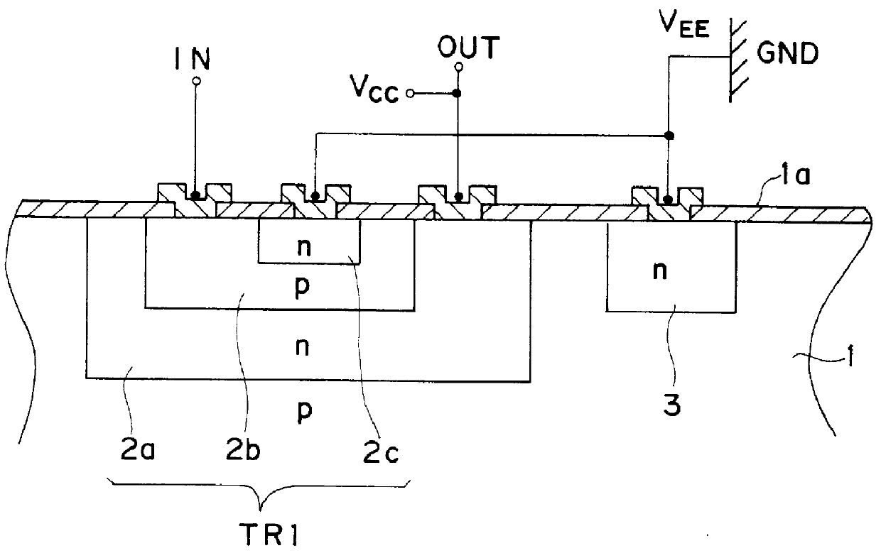
FIG. 3 is a schematic cross section of a semiconductor device provided with a planar bipolar transistor and a built-in ingredient acting as an element to protect the bipolar transistor from an external surge voltage e.g. an electrostatic surge voltage and the like, in accordance with a first embodiment of this invention,

Problems solved by technology

The foregoing semiconductor device provided with a bipolar transistor attached by a monolithic or built-in ingredient acting as a parasitic bipolar transistor for protecting the bipolar transistor from an external surge voltage is, however, involved with a drawback in which one or more parasitic capacitors is or are inevitably formed to be connected with the bipolar transistor.
These parasitic capacitors readily decrease the operation speed of the circuit including the bipolar transistor.

Method used


Image

  • Bipolar transistor with collector surge voltage protection
  • Bipolar transistor with collector surge voltage protection
  • Bipolar transistor with collector surge voltage protection

Examples


first embodiment

A planar bipolar transistor having a doped region having a conductivity opposite to that of a semiconductor substrate, the doped region being produced along the top surface of the semiconductor substrate at a location close to the bipolar transistor, and the emitter of the bipolar transistor being connected the doped region and a fixed potential (V.sub.EE) or the ground potential.

Referring to FIGS. 3 and 4, the top surface of a p-doped Si substrate (1) is oxidized to produce an SiO.sub.2 film (1a) thereon. After removing the SiO.sub.2 film (1a) from an area on which a collector is scheduled to be produced, an n-impurity is introduced into the top surface region of the Si substrate (1) to produce a collector (2a). After an annealing process is conducted to diffuse the n-impurity, another SiO.sub.2 film produced during the annealing process is removed from an area on which a base is scheduled to be produced. A p-impurity is introduced into the top surface region of the Si substrate (1...

second embodiment

A planar bipolar transistor surrounded by a doped region having a conductivity opposite to that of a semiconductor substrate.

Referring to FIGS. 9 and 10, a planar bipolar transistor (TR1) consisting of a collector (2a), a base (2b) and an emitter (2c) is surrounded by an n-doped region (4). As is illustrated in FIG. 3, an input signal (IN) is applied to the base (2b), and an output signal (OUT) is taken out of an output terminal (OUT) connected the collector (2a). The emitter (2c) is connected the fixed potential (V.sub.EE) or is grounded. Incidentally, it is connected the n-doped region (4), which surrounds the transistor (TR1) in this embodiment.

The operation of the semiconductor device provided with a planar bipolar transistor and a built-in ingredient acting as an element to protect the bipolar transistor from an external surge voltage e.g. an electrostatic surge voltage and the like in accordance with this second embodiment of this invention is entirely identical to that of the...

third embodiment

A planar bipolar transistor attached by two doped regions each of which is doped with an impurity having a conductivity opposite to that of a semiconductor substrate, the emitter of the bipolar transistor being connected with the one of the doped regions located close to the bipolar transistor (TR1) and a fixed potential (V.sub.EE) or the ground potential, the other one of the doped regions located remote from the bipolar transistor (TR1) being connected the positive power supply (V.sub.CC).

Referring to FIGS. 11, 12 and 13, a planar bipolar transistor consisting of a collector (2a), a base (2b) and an emitter (2c) is attached by two doped regions (3) and (5) each of which is doped with an n impurity or an impurity having a conductivity opposite to that of a p-doped Si substrate (1). The emitter (2c) is connected the first one of the n-doped regions (3) located close to the bipolar transistor (TR1) and the fixed potential (V.sub.EE) or the ground potential. The second one of the n-do...


PUM


Abstract

A semiconductor device provided with a planar bipolar transistor and a built-in ingredient acting as an element to protect the bipolar transistor from an external surge voltage e.g. an electrostatic surge voltage and the like, is provided with a planar bipolar transistor further provided with a doped region having a conductivity opposite to that of a semiconductor substrate in which the foregoing planar bipolar transistor is produced, the doped region being produced along the top surface of the semiconductor substrate at a location close to the bipolar transistor, and the emitter of the bipolar transistor being connected the doped region and a fixed potential (VEE) or the ground potential, whereby the operation speed of a circuit including the transistor is not reduced by potential parasitic capacitors which otherwise accompany the built-in ingredients produced to protect the transistor from an external surge voltage e.g. an electrostatic surge voltage and the like.

Description

This invention relates to a semiconductor device provided with a planar bipolar transistor and a built-in ingredient acting as an element to protect the bipolar transistor from an external surge voltage e.g. an electrostatic surge voltage and the like.BACKGROUND OF THE INVENTION AND PRIOR ART STATEMENTA transistor is often exposed to an external surge voltage e.g. an electrostatic surge voltage which is often generated in an IC or the like in which the transistor is employed, during a period in which the IC or the like is employed under environments where the IC or the like is rubbed with an insulator, resultantly electrostatic electricity is generated in and / or on the IC or the like. To protect the transistor from such an external surge voltage, an ingredient acting as an element to drive away the external voltage from the transistor or to cause the external voltage to bypass the transistor, is built in a semiconductor device in which the transistor is built as well.A brief descrip...

Claims


Application Information

Patent Timeline
Patent Type & Authority Patents(United States)
IPC IPC(8): H01L29/732H01L29/66H01L27/02H01L21/822H01L27/04H01L21/8222H01L27/06
CPCH01L27/0255H01L29/7322H01L27/08
Inventor SHIMIZU, TAKAYUKI
Owner LAPIS SEMICON CO LTD
Learn More