Systems and methods for high precision optical characterization of carrier transport properties in semiconductor manufacturing

a carrier transport and optical characterization technology, applied in the direction of measurement devices, instruments, material analysis, etc., can solve the problems of loss of manufacturing yield, device timing variability, and many process steps have the potential to alter or degrade such carrier transport properties, and achieve high precision optical characterization of carrier transport properties

Pending Publication Date: 2022-09-15
XCALIPR CORP
View PDF0 Cites 0 Cited by
  • Summary
  • Abstract
  • Description
  • Claims
  • Application Information

AI Technical Summary

Benefits of technology

[0012]The present invention relates to methods for determining electronic transport properties in a semiconductor sample. More particularly, the present invention provides methods for the direct, high precision optical characterization of carrier diffusion lengths, recombination lifetimes, and / or diffusion coefficients using Z-scanning laser photo-modulated reflectance techniques. Once these carrier properties are measured, various additional electronic transport properties including the carrier mobility, the carrier effective mass, and the sheet resistance may be evaluated with high precision. Thus high precision optical characterization of carrier transport properties is achieved.
[0014]A regressive fit to the PMR data is performed using a parametrized function wherein at least one carrier transport property is treated as a variable parameter. The error estimates on the output fit parameters depend upon the measurement uncertainties at each data point, the number and spacing of the data points, and the match of the analytic model to the data. The PMR measurement uncertainties approach the ppm level whereas the analytic model presented herein is broadly applicable. Thus in practice, the precision of the technique only depends upon the number and spacing of the data points in Z. In short, the analytic parametrization for the Z dependence of the PMR signal in terms of the complex diffusion length enables the direct, high precision determination of carrier diffusion lengths and / or recombination lifetimes using data obtained from a simple optical arrangement.
[0016]Furthermore, the Z-scanning laser PMR techniques disclosed here are fully applicable to PMR techniques which directly detect the excess carrier density (i.e. via the Drude effect). The experimentally measured PMR signal under such conditions is:ΔR / R=−q2λ2 / 2π2εsn(n2−1)mc2×ΔN,  (2)where n is index of refraction, m is the carrier effective mass, and ANis the pump induced excess carrier density [R. E. Wagner and A. Mandelis, “A Generalized Calculation of the Temperature and Drude Photo-Modulated Optical Reflectance Coefficients in Semiconductors,”J. Phys. Chem. Solids 52, 1061-1070 (1991).]. This Drude effect PMR signal is proportional to the square of the probe wavelength. Thus direct measurement of carrier modulation is preferred at longer wavelengths, such as, for example, in the near-TR. Such wavelengths generally penetrate far more deeply into the bulk and therefore do not provide the near surface specificity available when the wavelength of the probe is selected to coincide with interband transitions in the UV (i.e. such that the PMR signal arises from the Franz-Keldysh effect). Nevertheless, the ΔN factor present in the expression for the Drude effect PMR signal will exhibit the same spatial profile dependence on diffusion length as exhibited by the photo-voltage. In particular, the pump will induce an excess carrier density within the same radius of modulation as exhibited by ΔV. Thus the inventive techniques disclosed herein are fully applicable to PMR probe beam wavelengths selected to detect the excess carrier density via the Drude effect.

Problems solved by technology

In modern device manufacturing, many process steps have the potential to alter or degrade such carrier transport properties.
Spatial and temporal shifts in process conditions cause variations in carrier transport properties, resulting in device timing variability and loss of manufacturing yield.
Although these techniques have the requisite measurement capability, they are not suitable for in-line process control due to their destructive and time-consuming nature.
Such contact is disadvantageous in process control applications due to the possibility of particulate contamination.
However, in each case some particular feature of the technique presents a significant impediment to use for in-line process control.
For example, the capacitive probes used in SPV techniques suffer from limited sensitivity (e.g. from stray capacitances) and poor spatial resolution.
The spatial resolution of SPV limits its application to “at-line” process monitoring using unpatterned blanket wafers.
Another optical technique, THz spectroscopy, is sensitive to carrier mobility but requires a complicated (and expensive) experimental setup.
Despite these advances, PMR is not widely used to determine electronic transport properties in semiconductor manufacturing.
Thus in view of the appearance of the SPV in the PMR signal, the difficulties encountered in the use of SPV to determine carrier transport properties are likewise present in conventional PMR techniques.

Method used


Image

  • Systems and methods for high precision optical characterization of carrier transport properties in semiconductor manufacturing
  • Systems and methods for high precision optical characterization of carrier transport properties in semiconductor manufacturing
  • Systems and methods for high precision optical characterization of carrier transport properties in semiconductor manufacturing

Examples


Embodiment Construction

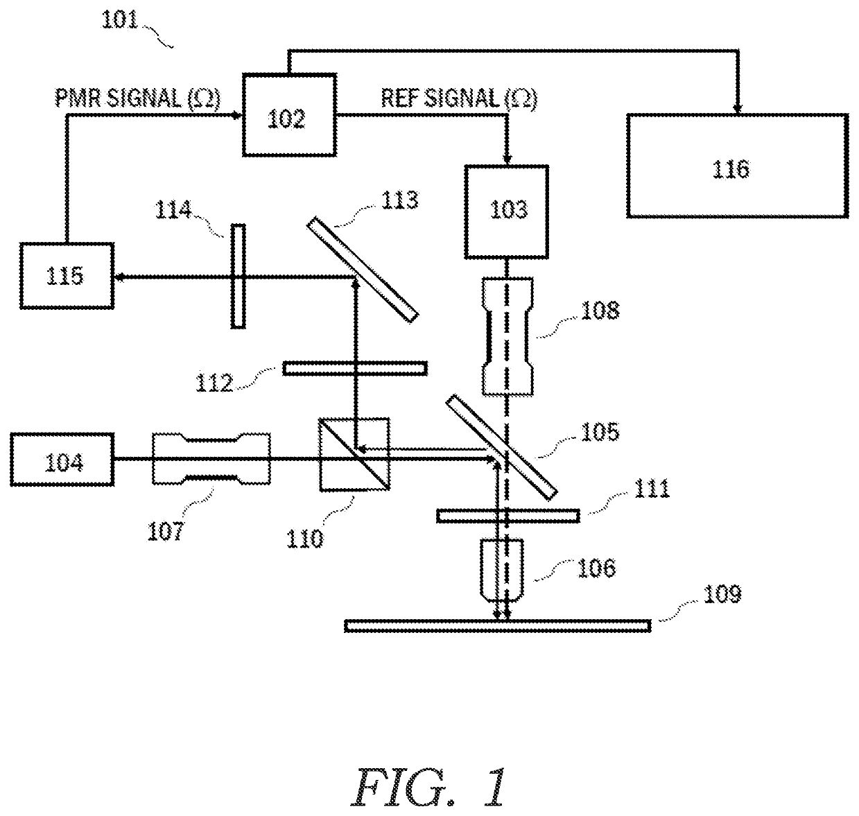
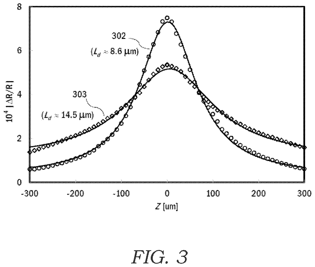
[0027]The following discusses embodiments of systems and methods of Z-scanning laser photo-modulated reflectance characterization of electronic transport properties in semiconductors. It is to be understood that the embodiments of systems and methods of the present description may be used to determine electronic transport properties in any semiconductor, the discussion of exemplary silicon semiconductors considered to be exemplary only and in no way limiting in scope. It should be appreciated that the present embodiments provide numerous applicable inventive concepts that may be embodied in a variety of specific contexts. The specific embodiments discussed herein are merely illustrative of specific ways to make and / or use the invention and are not intended to limit the scope of the claims.

[0028]The present embodiments are based upon profiling of the output signals of a laser PMR system as the sample is stepped through focus. Exemplary embodiments discussed herein use laser beams hav...


PUM

PropertyMeasurementUnit
wavelengthaaaaaaaaaa

Abstract

A precise optical technique for measuring electronic transport properties in semiconductors is disclosed. The sensitivity of the technique to electronic transport properties follows from a simple analytic expression for the Z dependence of a photo-modulated reflectance signal in terms of the (complex) carrier diffusion length. The sensitivity of the technique to electronic transport properties also enables a trained neural network to predict electronic transport properties directly from Z-scan photo-modulated reflectance data. Synthetic data and / or physical constraints may be derived from the analytical expression and incorporated into a machine learning algorithm. Moreover, electronic transport properties as determined or predicted may be used to enable machine learning based control of semiconductor process tools and / or manufacturing processes, including via advanced reinforcement learning algorithms.

Description

CROSS-REFERENCE TO RELATED PATENT APPLICATIONS[0001]The present application is a continuation-in-part of U.S. patent application Ser. No. 17 / 149,303, filed Jan. 14, 2021, which is a continuation of application Ser. No. 15 / 855,142, filed Dec. 27, 2017, now U.S. Pat. No. 10,921,369, which has benefit of priority of U.S. Provisional Patent Application No. 62 / 498,685, filed Jan. 5, 2017, each of which are herein incorporated in their entireties by this reference.BACKGROUNDField of the Invention[0002]The present invention relates to optical measurement of electronic transport properties in semiconductor manufacturing and, more particularly, to high precision measurement of carrier diffusion lengths, recombination lifetimes, diffusion coefficients, mobilities, and related carrier transport properties using photo-modulated reflectance techniques.Background of the Invention[0003]Semiconductor device performance depends fundamentally on the transport properties of electronic charge carriers ...

Claims


Application Information

Patent Timeline
Patent Type & Authority Applications(United States)
IPC IPC(8): G01R31/309G01R31/28
CPCG01R31/309G01R31/2831G01N21/1717G01N2021/1725
Inventor CHISM, II, WILLIAM W.
Owner XCALIPR CORP
Why Eureka
Try Eureka