Light-emitting device, light-emitting apparatus, electronic apparatus, and lighting device

a technology of light-emitting devices and electronic devices, which is applied in the direction of solid-state devices, semiconductor devices, organic compounds, etc., can solve the problems of increasing the driving voltage of the el device and increasing power consumption, and achieves high carrier-transport properties, improved outcoupling efficiency, and high refractive index

Pending Publication Date: 2022-03-10
SEMICON ENERGY LAB CO LTD
View PDF0 Cites 0 Cited by
  • Summary
  • Abstract
  • Description
  • Claims
  • Application Information

AI Technical Summary

Benefits of technology

[0007]It is possible to improve the outcoupling efficiency when the low-refractive-index layer is provided inside the organic EL device as described above; however, there is generally a trade-off relationship between a high carrier-transport property and a low refractive index. This is because the carrier-transport property of an organic compound largely depends on an unsaturated bond, and an organic compound having many unsaturated bonds tends to have a high refractive index.
[0009]When an organic EL device is manufactured using a material with a low carrier-transport property, the driving voltage of the EL device is increased, so that the power consumption is increased. The amount of power consumption of an organic EL device is extremely important because a battery is often used to drive the organic EL device owing to its features of being thin and lightweight.
[0010]In view of the above, an object of one embodiment of the present invention is to provide an organic compound that has a low refractive index and can inhibit an increase in driving voltage even when used in an EL device.
[0011]Another object of one embodiment of the present invention is to provide an organic compound with which a light-emitting device with high emission efficiency and low driving voltage can be manufactured. Another object of one embodiment of the present invention is to provide a light-emitting device with high emission efficiency and low driving voltage. Another object of one embodiment of the present invention is to provide any of a light-emitting device, a light-emitting apparatus, an electronic apparatus, a display device, and an electronic device each having low power consumption.
[0052]According to one embodiment of the present invention, an organic compound with which a light-emitting device with high emission efficiency and low driving voltage can be manufactured can be provided. According to another embodiment of the present invention, a light-emitting device with high emission efficiency and low driving voltage can be provided. According to another embodiment of the present invention, any of a light-emitting device, a light-emitting apparatus, an electronic apparatus, a display device, and an electronic device each having low power consumption can be provided.

Problems solved by technology

When an organic EL device is manufactured using a material with a low carrier-transport property, the driving voltage of the EL device is increased, so that the power consumption is increased.

Method used


Image

  • Light-emitting device, light-emitting apparatus, electronic apparatus, and lighting device
  • Light-emitting device, light-emitting apparatus, electronic apparatus, and lighting device
  • Light-emitting device, light-emitting apparatus, electronic apparatus, and lighting device

Examples


embodiment 1

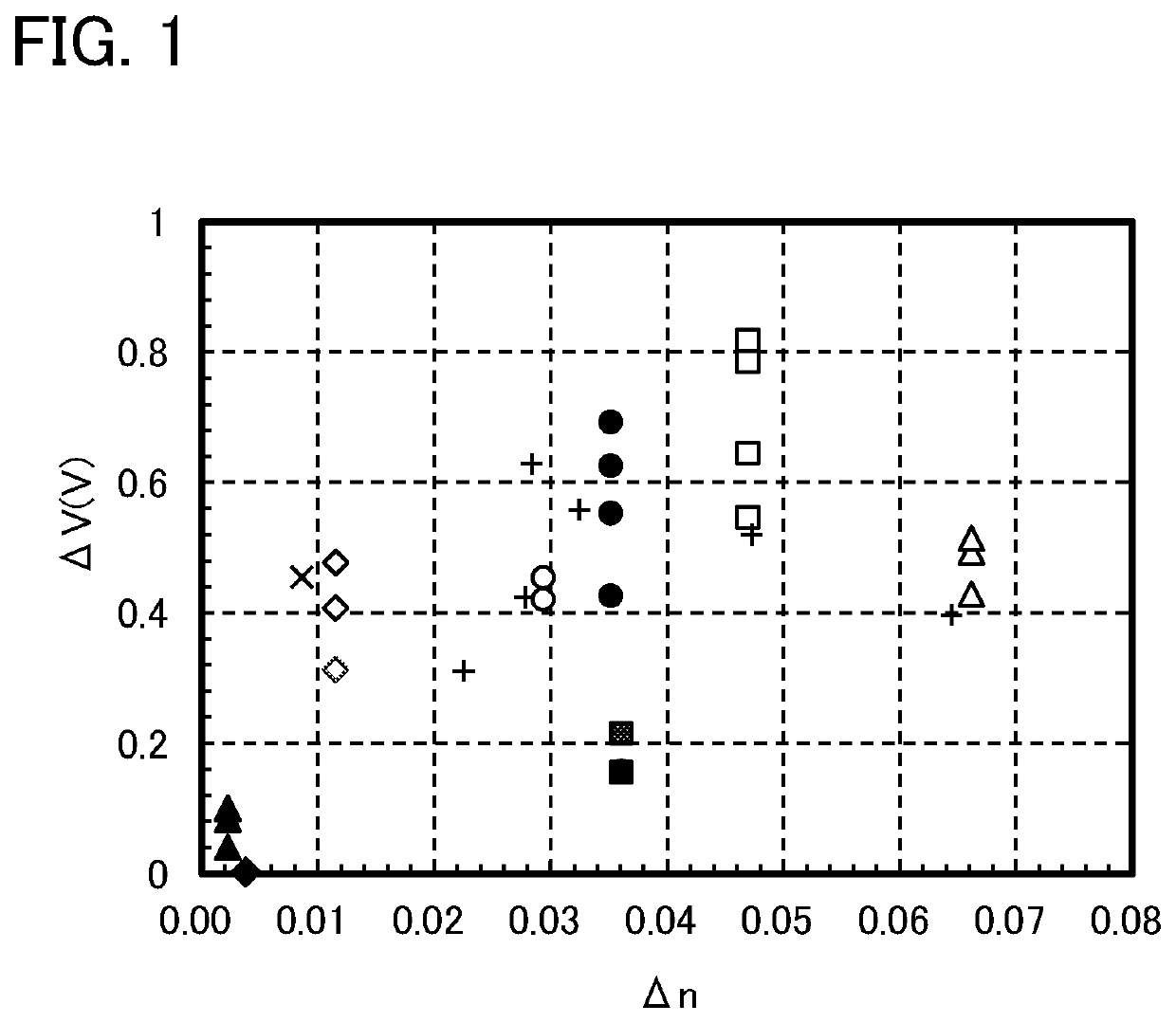
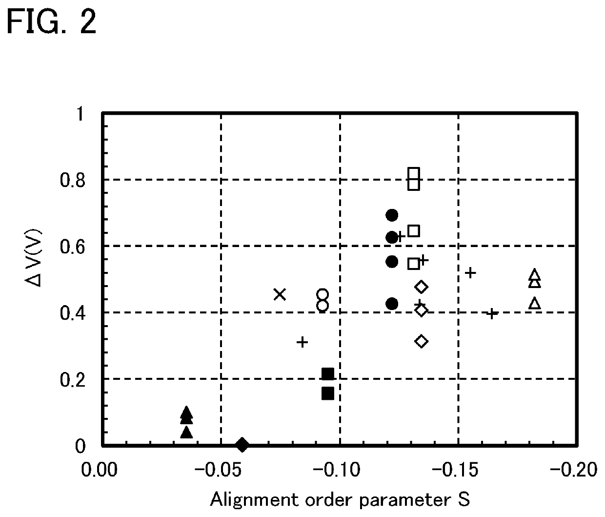
[0098]Of light entering a material perpendicularly to the light axis of the material, light with a plane of vibration perpendicular to the light axis is called ordinary light (an ordinary ray) and light with a plane of vibration parallel to the light axis is called extraordinary light (an extraordinary ray). An ordinary refractive index no and an extraordinary refractive index ne are refractive indices of a material to be measured with respect to ordinary light and extraordinary light. The ordinary refractive index no and the extraordinary refractive index ne can be calculated by anisotropic analysis. Birefringence (Δn) is expressed by the difference between the ordinary refractive index no and the extraordinary refractive index ne (Δn=|no−ne|). When a material has anisotropy, the refractive index no for ordinary light and the refractive index ne for extraordinary light sometimes differ from each other, and the difference is the birefringence Δn.

[0099]An organic compound of one embo...

embodiment 2

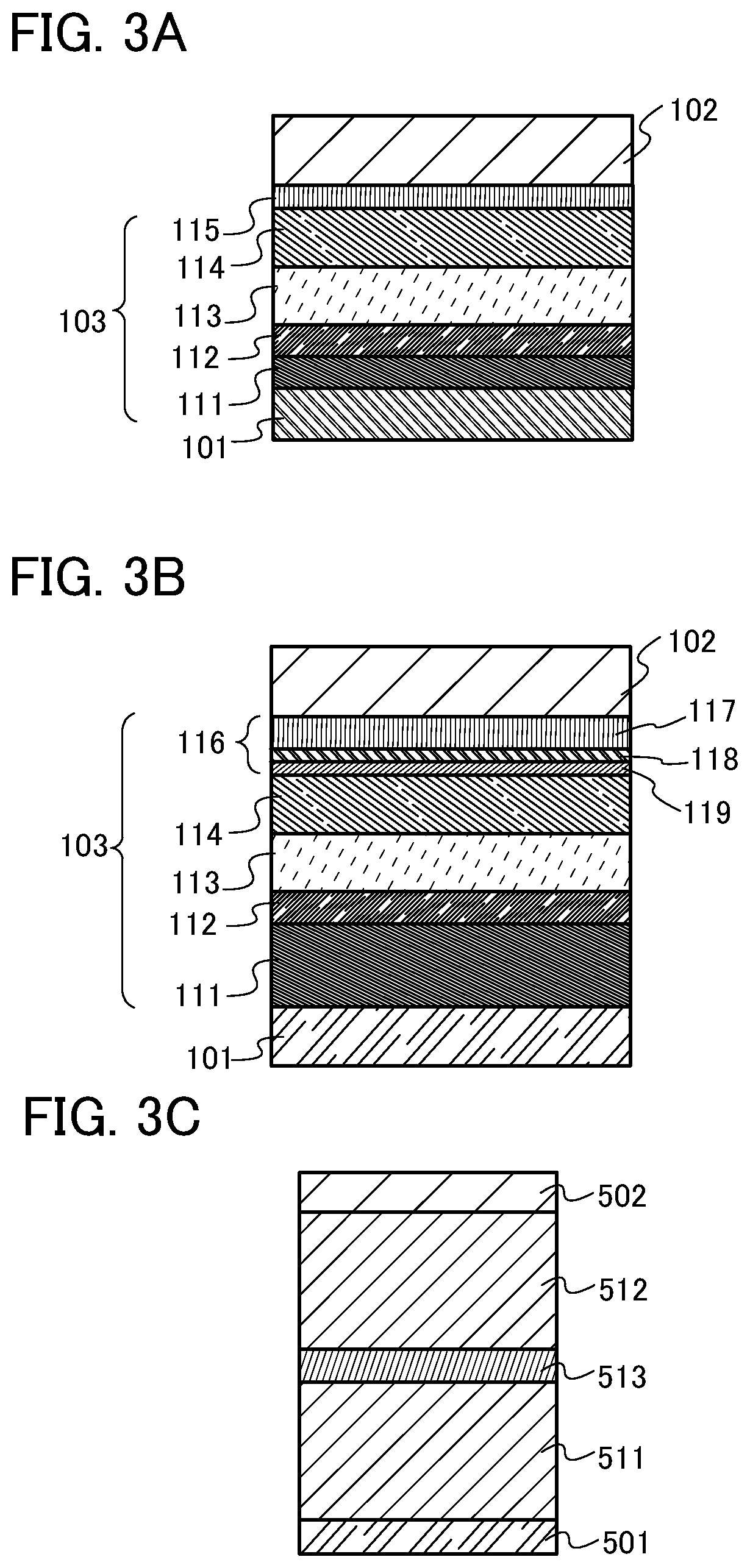
[0134]FIG. 3A illustrates a light-emitting device of one embodiment of the present invention. The light-emitting device of one embodiment of the present invention includes a first electrode 101, a second electrode 102, and an EL layer 103, and the organic compound described in Embodiment 1 is used for the EL layer.

[0135]The EL layer 103 includes a light-emitting layer 113 and may also include one or both of a hole-injection layer 111 and a hole-transport layer 112. The light-emitting layer 113 includes a light-emitting material, and light is emitted from the light-emitting material in the light-emitting device of one embodiment of the present invention. The light-emitting layer 113 may include a host material and other materials. The organic compound of one embodiment of the present invention described in Embodiment 1 may be included in any of the light-emitting layer 113, the hole-transport layer 112, and the hole-injection layer; alternatively, the organic compound may be included...

embodiment 3

[0207]In this embodiment, a light-emitting apparatus including the light-emitting device described in Embodiment 2 is described.

[0208]In this embodiment, the light-emitting apparatus manufactured using the light-emitting device described in Embodiment 2 is described with reference to FIGS. 4A and 4B. Note that FIG. 4A is a top view of the light-emitting apparatus and FIG. 4B is a cross-sectional view taken along the lines A-B and C-D in FIG. 4A. This light-emitting apparatus includes a driver circuit portion (source line driver circuit) 601, a pixel portion 602, and a driver circuit portion (gate line driver circuit) 603, which are to control light emission of a light-emitting device and illustrated with dotted lines. Reference numeral 604 denotes a sealing substrate; 605, a sealing material; and 607, a space surrounded by the sealing material 605.

[0209]Reference numeral 608 denotes a lead wiring for transmitting signals to be input to the source line driver circuit 601 and the gate...


PUM

PropertyMeasurementUnit
refractive indexaaaaaaaaaa
wavelengthaaaaaaaaaa

Abstract

A light-emitting device with high emission efficiency and low driving voltage is provided. A light-emitting apparatus, an electronic device, and a lighting device with low power consumption are provided. The following organic compound is provided: the organic compound has an arylamine structure; and when the organic compound is deposited to be a film, the ordinary refractive index of the deposited film with respect to light with a wavelength of 458 nm is greater than or equal to 1.50 and less than or equal to 1.75, the birefringence Δn of the deposited film with respect to light with a wavelength of 458 nm is greater than or equal to 0 and less than or equal to 0.008, or the alignment order parameter of the deposited film with respect to light with a wavelength corresponding to the longest wavelength where an absorption peak appears in the absorption spectrum is greater than or equal to −0.07 and less than or equal to 0.00.

Description

BACKGROUND OF THE INVENTION1. Field of the Invention[0001]One embodiment of the present invention relates to an organic compound, a light-emitting element, a light-emitting device, a display module, a lighting module, a display device, a light-emitting apparatus, an electronic apparatus, a lighting device, and an electronic device. Note that one embodiment of the present invention is not limited to the above technical field. The technical field of one embodiment of the invention disclosed in this specification and the like relates to an object, a method, or a manufacturing method. One embodiment of the present invention relates to a process, a machine, manufacture, or a composition of matter. Specifically, examples of the technical field of one embodiment of the present invention disclosed in this specification include a semiconductor device, a display device, a liquid crystal display device, a light-emitting apparatus, a lighting device, a power storage device, a memory device, an ...

Claims


Application Information

Patent Timeline
Patent Type & Authority Applications(United States)
IPC IPC(8): H01L51/00C07C211/61
CPCH01L51/006H01L51/5056C07C211/61H10K59/12H10K85/633H10K85/6574H10K50/15H10K50/17H10K59/00H10K85/615H10K85/6572C07C2601/14C07C2603/18
Inventor OHSAWA, NOBUHARUSEO, SATOSHIWATABE, TAKEYOSHIUEDA, AIRIKUBOTA, TOMOHIROHIRAHARA, TAKASHI
Owner SEMICON ENERGY LAB CO LTD
Why Eureka
Try Eureka