System for measuring junction temperature of photonics devices

Pending Publication Date: 2022-03-10
OZYEGIN UNIVSI
View PDF0 Cites 0 Cited by
  • Summary
  • Abstract
  • Description
  • Claims
  • Application Information

AI Technical Summary

Benefits of technology

The present invention is a control system that uses temperature sensors to measure the temperature of photonics devices. The system collects data from multiple sensors, converts it into digital data, and sends feedback to the power supply to regulate the temperature. The system is user-friendly and reduces measurement time, resulting in accurate results. Additionally, the system includes a robotic arm that makes it easy to measure multi-chip LED devices by applying current / voltage individually to each chip. The control system allows the user to customize their measurement plan for each device. Overall, the invention simplifies the measurement process and reduces the time required for the user.

Problems solved by technology

As electronic packages are getting smaller day by day, generated heat fluxes are also becoming more intense and causes serious lifetime and performance issues on consumer devices.
Although the light output of photonic devices is more efficient than the counterparts, they still dissipate about 80% of their energy input as heat.
However, existing temperature measurement devices are quite expensive for most of the device manufacturers, thermal engineers and designers who need to measure only the junction temperature of devices.
This technique involves a thermal characterization technique with high sampling rate and resolution of data collection, such as heat flow path construction, die attach qualification, and material property identification, all of which make the product quite expensive.
However, in various types of devices, there are thermal masses on top of the photonic module such as phosphor and attached lens that change the heat flux symmetry.
This issue brings difficulties for the interpretation of the structural function and leads to limitations especially for the coated devices such as white photonic products and etc.
In addition, thermal resistance of this material should be known or measured since the existence of this material in measurement technique affects the measurement results and brings additional uncertainty.

Method used


Image

  • System for measuring junction temperature of photonics devices
  • System for measuring junction temperature of photonics devices

Examples


Embodiment Construction

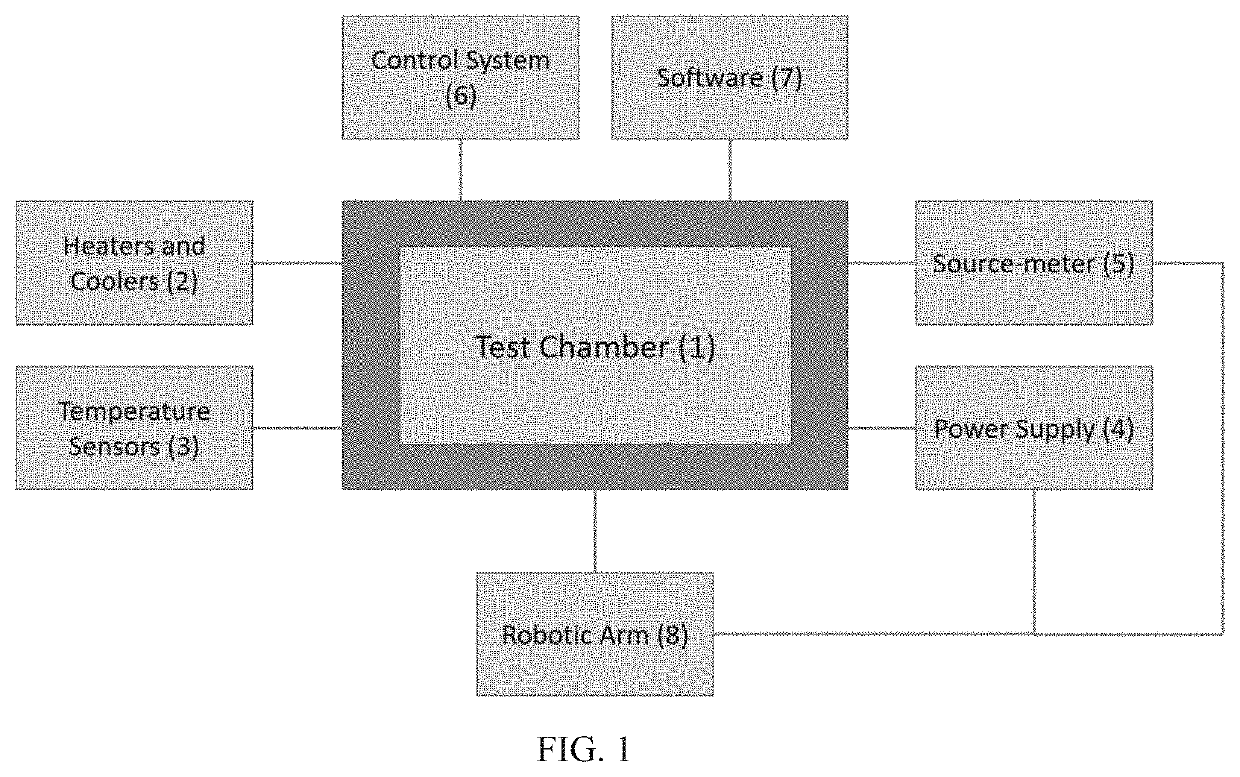
[0029]The present invention provides a system and a method for measuring the junction temperature of photonics which is the most vital need for the design of photonics products. The present invention also provides a temperature controlled environment for other purposes with a sensitive controller beyond measuring the junction temperature.

[0030]The system provided by the present invention is especially useful in photonics technologies, particularly in the research and development activities on the optical, electrical and thermal designs of photonics systems (e.g. LEDs).

[0031]In one embodiment of the present invention, the system for measuring the junction temperature of photonics comprises a test chamber (1), at least one heater (2), at least one temperature sensor(3), a power supply (4), a source-meter (5), a control system (6), a software package (7) and a robotic arm (8). In another embodiment of the present invention said system further comprises at least one cooler.
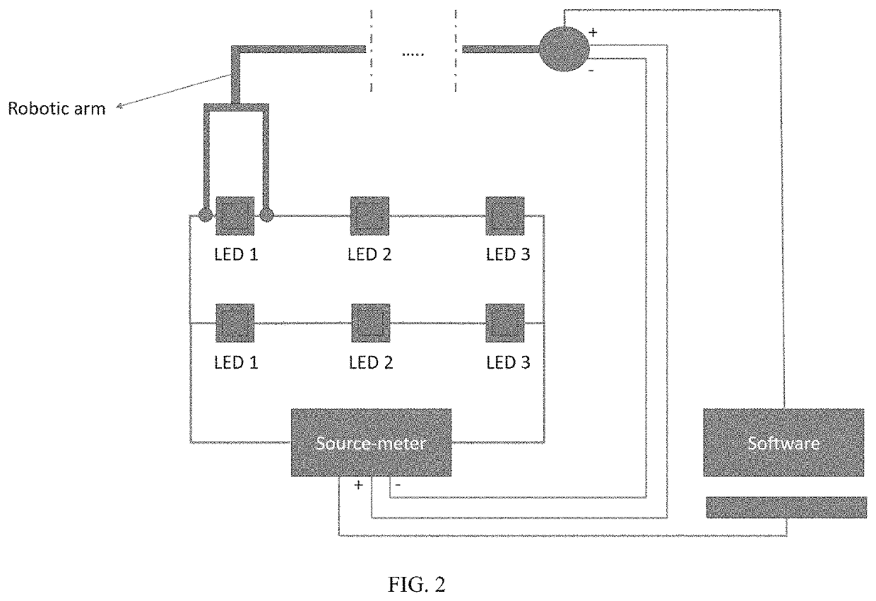
[0032]Test ch...


PUM


Abstract

A system for measuring the junction temperature of a photonics device comprising a) a test chamber, wherein a photonics device to be tested is placed inside, b) at least one heater, c) at least one temperature sensor, d) a source-meter configured to apply a driving current to the photonics device in order to read the corresponding forward voltage value at that temperature, e) a power supply, f) a control system and g) a software configured to start and control the measurements with either predefined default settings or the settings entered by the user.

Description

TECHNICAL FIELD OF THE INVENTION[0001]The present invention relates to a system and a method for measuring junction temperature of photonics devices such as light emitting diodes and lasers.BACKGROUND OF THE INVENTION[0002]As electronic packages are getting smaller day by day, generated heat fluxes are also becoming more intense and causes serious lifetime and performance issues on consumer devices. Light emitting diodes as photonic devices are also one of these photonics products and they are the future of display and lighting industry. Although the light output of photonic devices is more efficient than the counterparts, they still dissipate about 80% of their energy input as heat. In other words, only about 20% of the energy is converted into visible light.[0003]Photonic devices of the present invention like other photonics devices (lasers, vcsels etc) are semiconductor diodes which consist of two semiconductor materials called N-type and P-type. The interface between these two t...

Claims


Application Information

Patent Timeline
IPC IPC(8): G01K7/01G01K15/00
CPCG01K7/01G01K2217/00G01K15/005
Inventor ARIK, MEHMETTAMDOGAN, ENESOZLUK, BURAKMUSLU, AHMET METE
Owner OZYEGIN UNIVSI
Why Eureka
Try Eureka