Semiconductor structure and method for forming the same

Active Publication Date: 2022-01-27
SEMICON MFG INT (SHANGHAI) CORP +1
View PDF2 Cites 0 Cited by
  • Summary
  • Abstract
  • Description
  • Claims
  • Application Information

AI Technical Summary

Benefits of technology

The present invention provides a method for forming a semiconductor structure with improved efficiency. The method includes a step of removing a mask layer on a dummy device region and a source-drain plug, using the remaining mask layer on the gate structures as a mask. This simplifies the formation process and improves the efficiency of forming the semiconductor structure. Additionally, a dielectric layer is formed in the gate groove and the source-drain groove in the same step, which can block the gate structures and the source-drain plug simultaneously.

Problems solved by technology

Such a development trend makes the wafer surface unable to provide a sufficient area for fabricating required interconnection lines.

Method used


Image

  • Semiconductor structure and method for forming the same
  • Semiconductor structure and method for forming the same
  • Semiconductor structure and method for forming the same

Examples


Embodiment Construction

[0030]As will be appreciated from the background, currently, formed device still have poor performance problems. Reasons for the poor performance of the devices are analyzed now in combination with a method for forming a semiconductor structure.

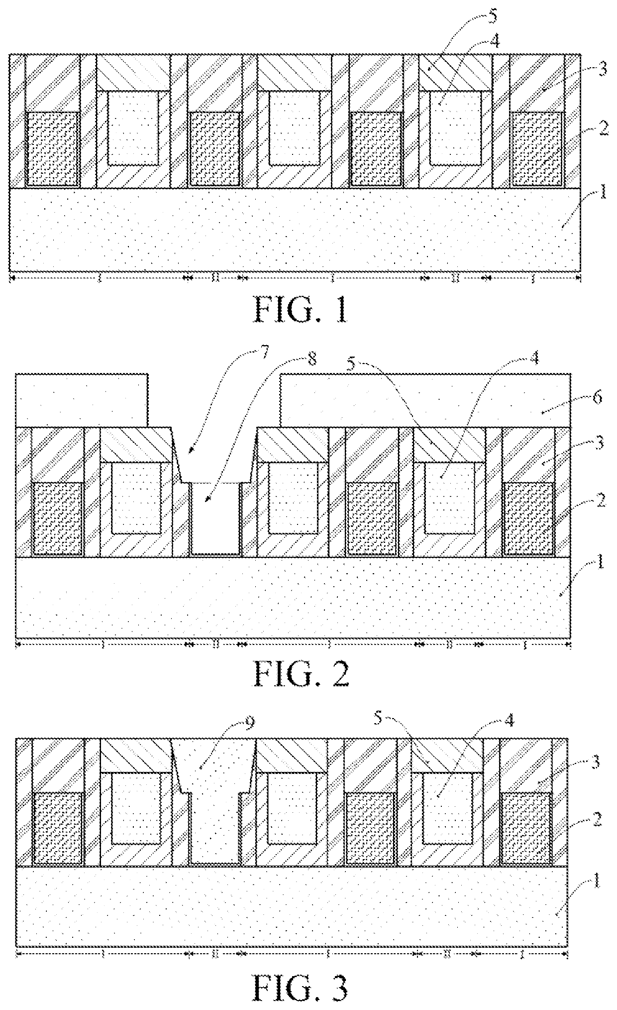
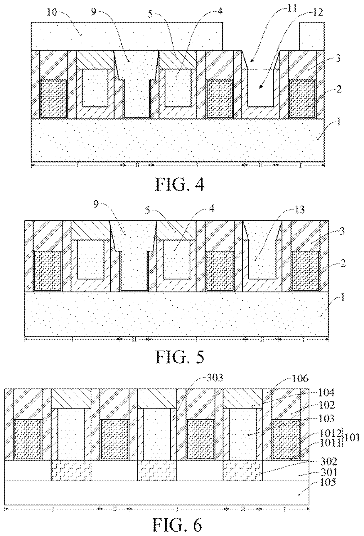
[0031]FIG. 1 to FIG. 5 are schematic structural diagrams corresponding to all steps in a method for forming a semiconductor structure.

[0032]As shown in FIG. 1, a base is provided. The base includes a device region I and a dummy device region II. The base includes an isolation layer 1, gate structures 2 located on the isolation layer 1, a first mask layer 3 located on the gate structures 2, a source-drain plug 4 located between the gate structures 2 and on the isolation layer 1, and a second mask layer 5 located on the source-drain plug 4.

[0033]As shown in FIG. 2, a first shielding layer 6 exposing the first mask layer 3 in the dummy device region II is formed. The first mask layer 3 on the gate structures 2 of the dummy device region II is re...


PUM


Abstract

A semiconductor structure and a method for forming the same are provided. One form of a forming method includes: providing a base, the base including a device region and a dummy device region, the base including an isolation layer, gate structures located on the isolation layer, a first mask layer located on the gate structures, a source-drain plug located between the gate structures and on the isolation layer, and a second mask layer located on the source-drain plug. In implementations of the present disclosure, the first mask layer and the second mask layer on the dummy device region are separately removed. Correspondingly, the first opening and the second opening respectively expose the gate structures and the source-drain plug in the dummy device region. The gate structures exposed by the first opening and the source-drain plug exposed by the second opening are removed in the same step. The gate groove at the bottom of the first opening and the source-drain groove at the bottom of the second opening are formed at the same time. Correspondingly, a dielectric layer may be formed in the gate groove and the source-drain groove in the same step. The dielectric layer may block the gate structures and the source-drain plug at the same time. This is advantageous for simplifying the formation process of the semiconductor structure.

Description

RELATED APPLICATIONS[0001]The present application claims priority to Chinese Patent Appln. No. 202010725785.4, filed Jul. 24, 2020, the entire disclosure of which is hereby incorporated by reference.BACKGROUNDTechnical Field[0002]Embodiments and implementations of the present disclosure relate to the field of semiconductor manufacturing, and in particular, to a semiconductor structure and a method for forming the same.Related Art[0003]With the continuous development of integrated circuit manufacturing technologies, people have increasingly high requirements on the integration level and performance of integrated circuits. To improve the integration level and reduce costs, critical dimensions of the components are continuously reduced, and the circuit density inside the integrated circuit is becoming increasingly high. Such a development trend makes the wafer surface unable to provide a sufficient area for fabricating required interconnection lines.[0004]To meet the requirement of the...

Claims


Application Information

Patent Timeline
IPC IPC(8): H01L29/417H01L29/40H01L29/66H01L29/06H01L21/033
CPCH01L29/41775H01L29/41791H01L21/0332H01L29/66545H01L29/0653H01L29/401H01L21/823431H01L21/823418H01L21/823437H01L21/823475H01L27/0886H01L21/31116H01L29/41783H01L29/7848
Inventor WANG, NAN
Owner SEMICON MFG INT (SHANGHAI) CORP
Why Eureka
Try Eureka