Flexible connection member and electronic device comprising same

Active Publication Date: 2021-10-21
SAMSUNG ELECTRONICS CO LTD +1
View PDF0 Cites 0 Cited by
  • Summary
  • Abstract
  • Description
  • Claims
  • Application Information

AI Technical Summary

Benefits of technology

The invention provides a flexible connection member that prevents signal degradation and loss due to impedance variations when the flexible circuit board is bent or deformed. The flexible connection member includes a bonding sheet between conductive layers that reduces RF impedance variations and improves RF signal integrity and stability. The invention also addresses the issue of reverse bending that leads to increased loss due to impance variations in high-speed signal lines, such as RF lines. The flexible connection member helps mitigate noise and stabilize signal integrity and RFI in electronic devices.

Problems solved by technology

When the structure is bent or deformed, some specific layers may be reversely bent due to a lack of inter-layer bonding in the multi-layered flexible circuit board.
The reverse bending may increase loss due to impedance variations in the case where the flexible circuit board region has a high-speed wiring signal line (e.g., an RF signal line).

Method used


Image

  • Flexible connection member and electronic device comprising same
  • Flexible connection member and electronic device comprising same
  • Flexible connection member and electronic device comprising same

Examples


Embodiment Construction

[0035]Hereinafter, embodiments of the disclosure are described with reference to the accompanying drawings.

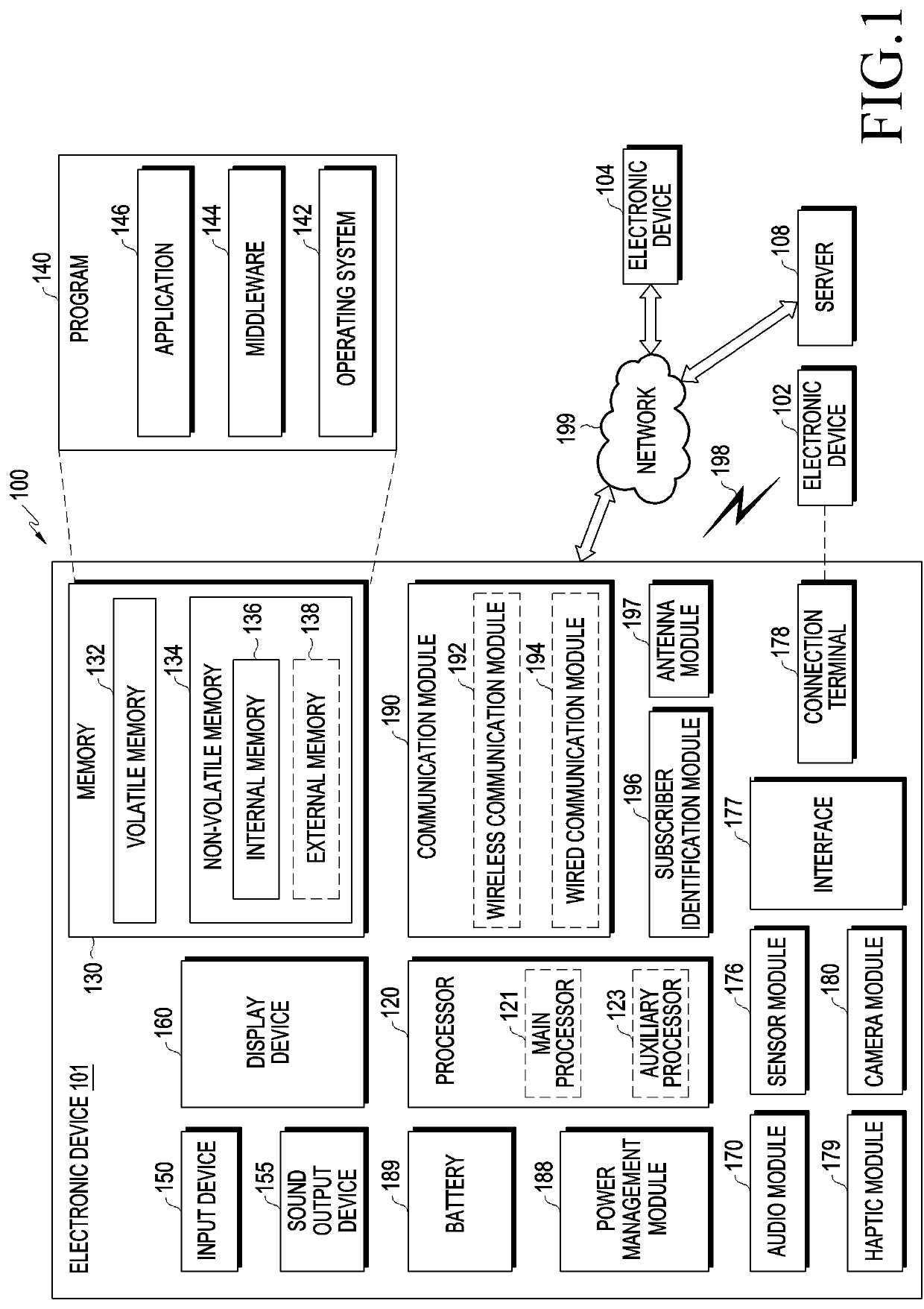
[0036]FIG. 1 is a block diagram illustrating an electronic device 101 in a network environment 100 according to various embodiments. Referring to FIG. 1, the electronic device 101 in the network environment 100 may communicate with an electronic device 102 via a first network 198 (e.g., a short-range wireless communication network), or an electronic device 104 or a server 108 via a second network 199 (e.g., a long-range wireless communication network). According to an embodiment, the electronic device 101 may communicate with the electronic device 104 via the server 108. According to an embodiment, the electronic device 101 may include a processor 120, memory 130, an input device 150, a sound output device 155, a display device 160, an audio module 170, a sensor module 176, an interface 177, a haptic module 179, a camera module 180, a power management module 188, a battery 189,...


PUM


Abstract

Various embodiments disclosed in the disclosure relate to a flexible connection member and an electronic device comprising same, the flexible connection member having an RF line for signal transmission formed therein, wherein an impedance of the RF line is prevented from being changed even when a flexible printed circuit board is bent. According to one embodiment, a connection member may be provided, the connection member comprising, a first conductive layer including a first logic line, and a second conductive layer in contact with the first conductive layer and including a bonding sheet layer, wherein the second conductive layer includes, a second logic line formed on part of the second conductive layer, and an RF line formed on other part of the second conductive layer, the bonding sheet layer includes, the second conductive layer adhered over the second logic line and the RF line, a first insulating layer formed between the first conductive layer and the second conductive layer, and pins formed on one side of the first conductive layer and the second conductive layer and configured to be electrically connected to connection pins of an external module, and the second conductive layer includes at least one via formed between the second logic line and the RF line so as to energize between the layers included in the second conductive layer. Such a flexible connection member may vary according to embodiments, and an electronic device comprising the flexible connection member may be provided according to various other embodiments.

Description

CROSS-REFERENCE TO RELATED APPLICATION(S)[0001]This application is a National Phase Entry of PCT International Application No. PCT / KR2019 / 010124, which was filed on Aug. 9, 2019, and claims priority to a Korean Patent Application No. 10-2018-0095168, which was filed on Aug. 14, 2018, in the Korean Intellectual Property Office, the contents of which are incorporated herein by reference.BACKGROUND1. Field[0002]Various embodiments disclosed in the disclosure relate to a flexible connection member having a line for transmitting an RF signal, and an electronic device including the same, in which the impedance of an RF line is prevented from being changed even when a structure is bent.2. Description of the Related Art[0003]Circuit boards may be divided into rigid circuit boards and flexible circuit boards according to their physical characteristics. Recently being used are rigid-flexible circuit boards which are a combination of rigid circuit board and flexible circuit board to enhance th...

Claims


Application Information

Patent Timeline
IPC IPC(8): H05K1/11H05K1/02H05K1/14
CPCH05K1/118H05K1/147H05K1/0237H05K1/0219H04M1/02H05K1/028H05K1/025H05K1/115
Inventor PARK, SUNGWONKIM, JUNGHYUBJEONG, HWANYOULLEE, SEUNGYUPLEE, YOUNGSUNJUNG, HESUKHONG, EUNSEOK
Owner SAMSUNG ELECTRONICS CO LTD
Why Eureka
Try Eureka