
Pixel interpolation device and pixel interpolation method, and image processing device, and program and recording medium

a technology of pixel interpolation and interpolation method, which is applied in the direction of image enhancement, picture signal generator, instruments, etc., can solve the problems of incorrect or unreliable pixel value of pixel signal obtained by reading through the use of photoelectric conversion elements, and achieve the effect of relatively small data processing amount and storage capacity

Active Publication Date: 2021-09-02
MITSUBISHI ELECTRIC CORP
View PDF13 Cites 0 Cited by
  • Summary
  • Abstract
  • Description
  • Claims
  • Application Information

AI Technical Summary

Benefits of technology

The present invention allows for interpolation without making the interpolated pixel look unnatural, while also requiring less storage capacity and data processing.

Problems solved by technology

Also, there are situations in which the pixel value of a pixel signal obtained by reading by means of a photoelectric conversion element is incorrect or unreliable for reasons such as irregularity of the photoelectric conversion element in the sensor chip, or smear of a part which is positioned in the optical path between the photoelectric conversion element in the sensor chip and the original, and which should be transparent.

Method used


Image

  • Pixel interpolation device and pixel interpolation method, and image processing device, and program and recording medium
  • Pixel interpolation device and pixel interpolation method, and image processing device, and program and recording medium
  • Pixel interpolation device and pixel interpolation method, and image processing device, and program and recording medium

Examples


first embodiment

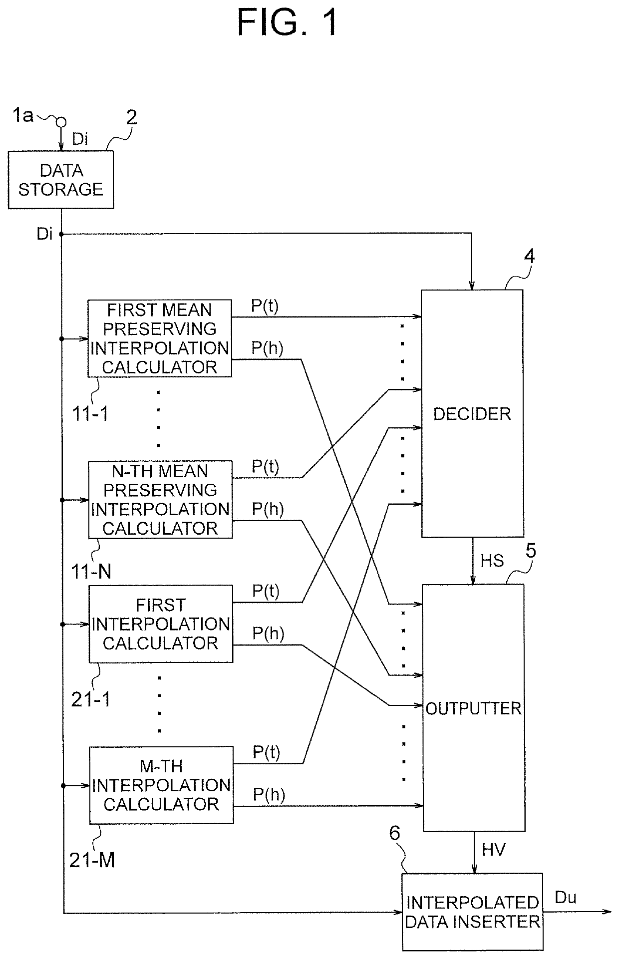
[0034]FIG. 1 is a functional block diagram schematically showing a configuration of a pixel interpolation device 1 of a first embodiment of the present invention.

[0035]The pixel interpolation device 1 interpolates pixel values of missing pixels in an image represented by image data Di supplied to an input terminal 1a.

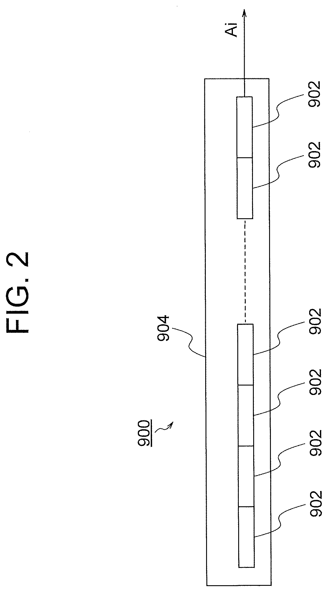
[0036]The image data Di is obtained, for example, by reading an object to be read (original) by means of an imaging device provided with a contact image sensor 900 shown in FIG. 2.

[0037]The contact image sensor 900 shown in FIG. 2 is formed by arranging a plurality of sensor chips 902 in a line on a board 904, and joining them together. The longitudinal direction of the contact image sensor 900 will be the main scanning direction.

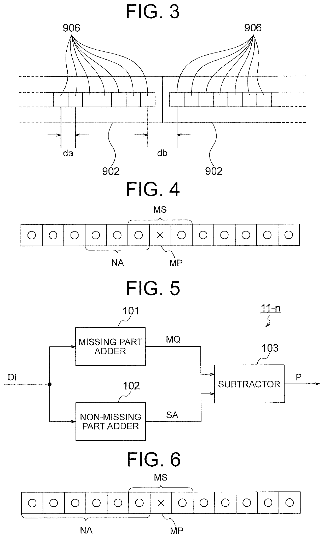
[0038]FIG. 3 shows, in detail, a joint part between mutually adjacent sensor chips 902.

[0039]As illustrated, each of the sensor chips 902 has a plurality of photo-electric conversion elements 906.

[0040]In each sensor chip 902, the plurality of...

second embodiment

[0108]The overall configuration of the pixel interpolation device 1 according to a second embodiment is as shown in FIG. 1.

[0109]The second embodiment differs from the first embodiment in the content of the process performed in each of the mean preserving interpolation calculators 11-1 to 11-N.

[0110]In the first embodiment, the number of pixels in the missing part and the number of pixels in the non-missing part which are referenced in the interpolation by each mean preserving interpolation calculator 11-n are equal to each other. In the second embodiment, the number of pixels in the non-missing part is larger than the number of pixels in the missing part.

[0111]FIG. 6 shows part of the input image Di, and indicates the positions of the pixels referenced in the interpolation by the mean preserving interpolation calculator 11-n in the present embodiment.

[0112]As in FIG. 4, the position of the missing pixel MP in the input image Di is assumed to be known in advance. The non-missing pix...

third embodiment

[0131]A pixel interpolation device 1c according to a third embodiment has a configuration generally as shown in FIG. 8.

[0132]The pixel interpolation device 1c shown in FIG. 8 is generally identical to the pixel interpolation device 1 in FIG. 1, but differs on the following points.

[0133]That is, in place of the mean preserving interpolation calculators 11-1 to 11-N in FIG. 1, mean preserving interpolation calculators 13-1 to 13-N are provided.

[0134]The first to N-th mean preserving interpolation calculators 13-1 to 13-N all perform the mean preserving interpolation calculation, but differ from each other in the number of pixels referenced in the interpolation.

[0135]Each of the first to N-th mean preserving interpolation calculators 13-1 to 13-N, i.e., the n-th mean preserving interpolation calculator 13-n, is similar to the n-th mean preserving interpolation calculator 11-n in the first embodiment, but differs in the arrangement of the pixels referenced in the interpolation, and has ...


PUM


Abstract

A first group of interpolation calculators performing interpolation by mean preserving interpolation calculation, and a second group of interpolation calculators performing interpolation by interpolation other than the mean preserving interpolation calculation are provided. Each of the interpolation calculators performs interpolation calculation for the missing pixel to calculate an interpolation candidate value (M(h)), and calculates test interpolation values (M(t)) treating pixels in a vicinity of the missing pixel as test pixels. A decider (4) selects one of the plurality of interpolation calculators based on results of the test interpolation. An outputter (5) selects the interpolation candidate value outputted from the interpolation calculator selected by the decider (4), among the plurality of interpolation candidate values (M(h)), and outputs the selected interpolation candidate value. Interpolation can be performed such that the interpolated pixel does not look unnatural, and yet the storage capacity and the data processing amount that are required are relatively small.

Description

TECHNICAL FIELD[0001]The present invention relates to a pixel interpolation device and a pixel interpolation method, and an image processing device, and a program and a recording medium.BACKGROUND ART[0002]An image reading device has been realized in which an object to be read (original) is read by a one-dimensional imaging device (line sensor), and image data corresponding to the original is generated. Line sensors in which a plurality of sensor chips each having a plurality of photoelectric conversion elements are aligned in the longitudinal direction of the line sensor, and are joined together are widely used.[0003]The sensor chips are formed by semiconductor manufacturing technology, so that the intervals between photoelectric conversion elements are relatively small. In contrast, the line sensor is manufactured by joining a plurality of sensor chips and fixing them on a board, or in a similar method. Accordingly, the interval between the photoelectric conversion elements positi...

Claims


Application Information

Patent Timeline
Patent Type & Authority Applications(United States)
IPC IPC(8): G06T5/00G06T3/40H04N9/04
CPCG06T5/002H04N2209/046H04N9/04515G06T3/4007H04N1/193H04N1/401G06T5/77H04N23/843G06T5/70
Inventor AOKI, TORUSUGANO, MIKIASAMURA, MASAKOTOYODA, YOSHITAKAKURIHARA, KOHEISUZUKI, DAISUKE
Owner MITSUBISHI ELECTRIC CORP
Learn More