Pixel array substrate
a technology of pixel array and substrate, which is applied in the field of display technology, can solve the problems of inability to achieve the narrow bezel design of the display panel, and the layout space of the circuit in the peripheral area is significantly reduced, and achieves the effect of narrow peripheral and better design margin for bonding pads
- Summary
- Abstract
- Description
- Claims
- Application Information
AI Technical Summary
Benefits of technology
Problems solved by technology
Method used
Image

Examples
first embodiment
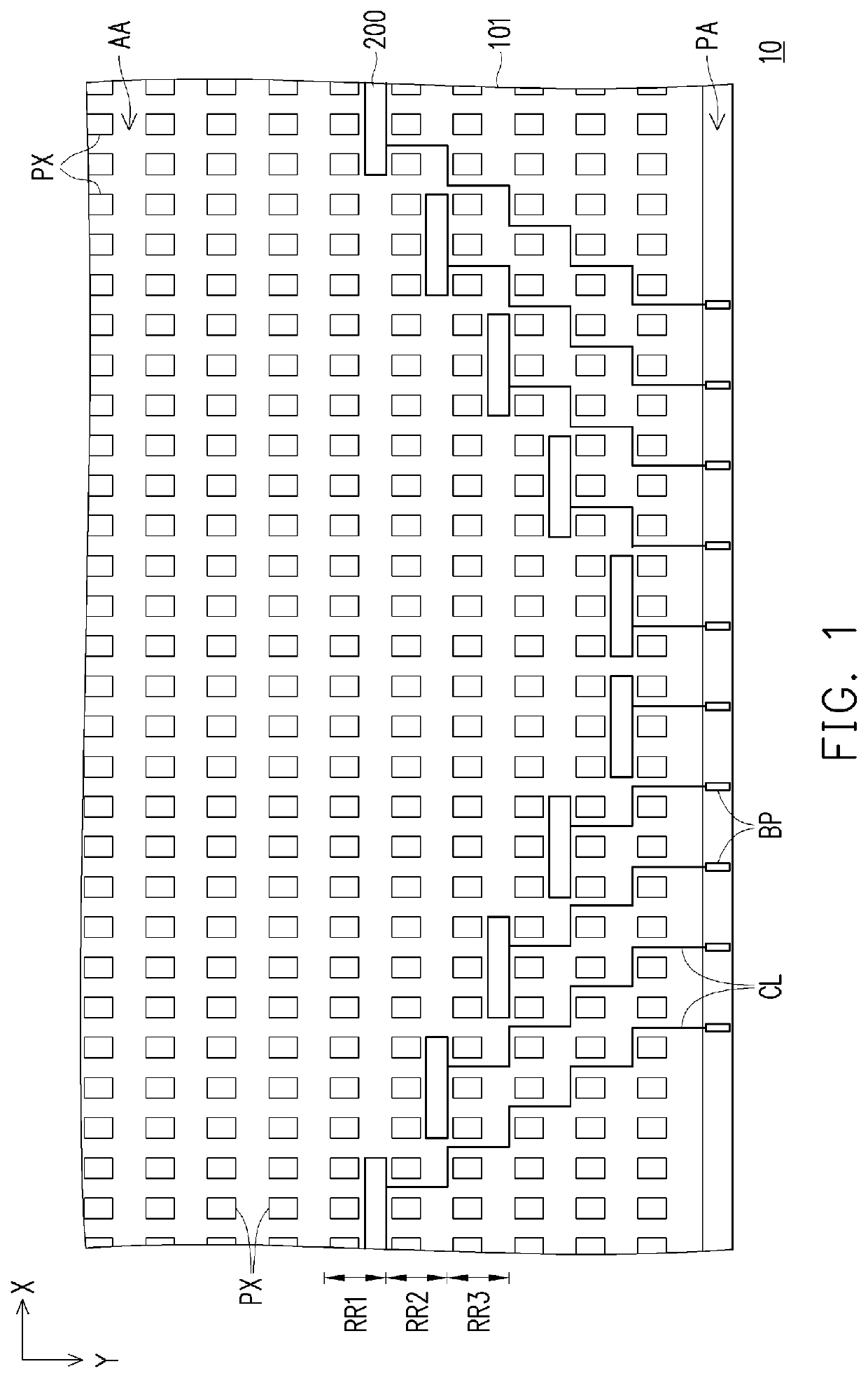
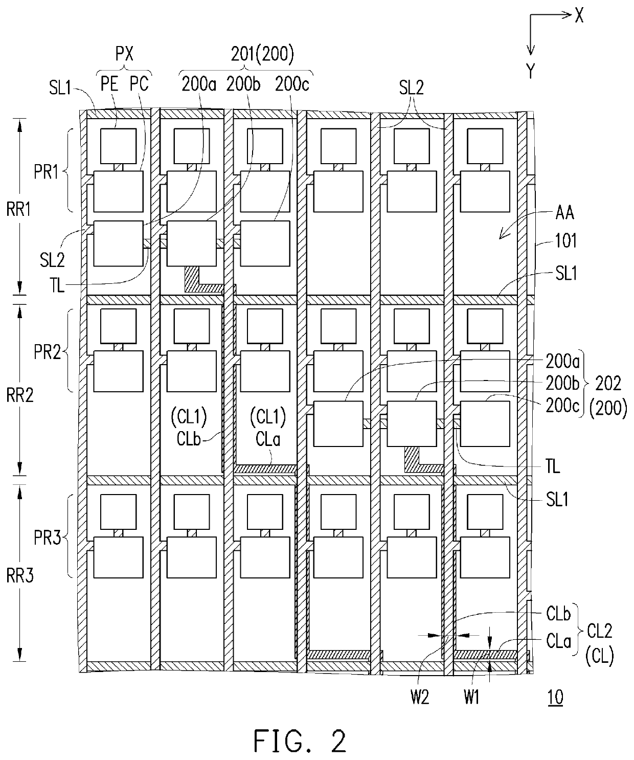
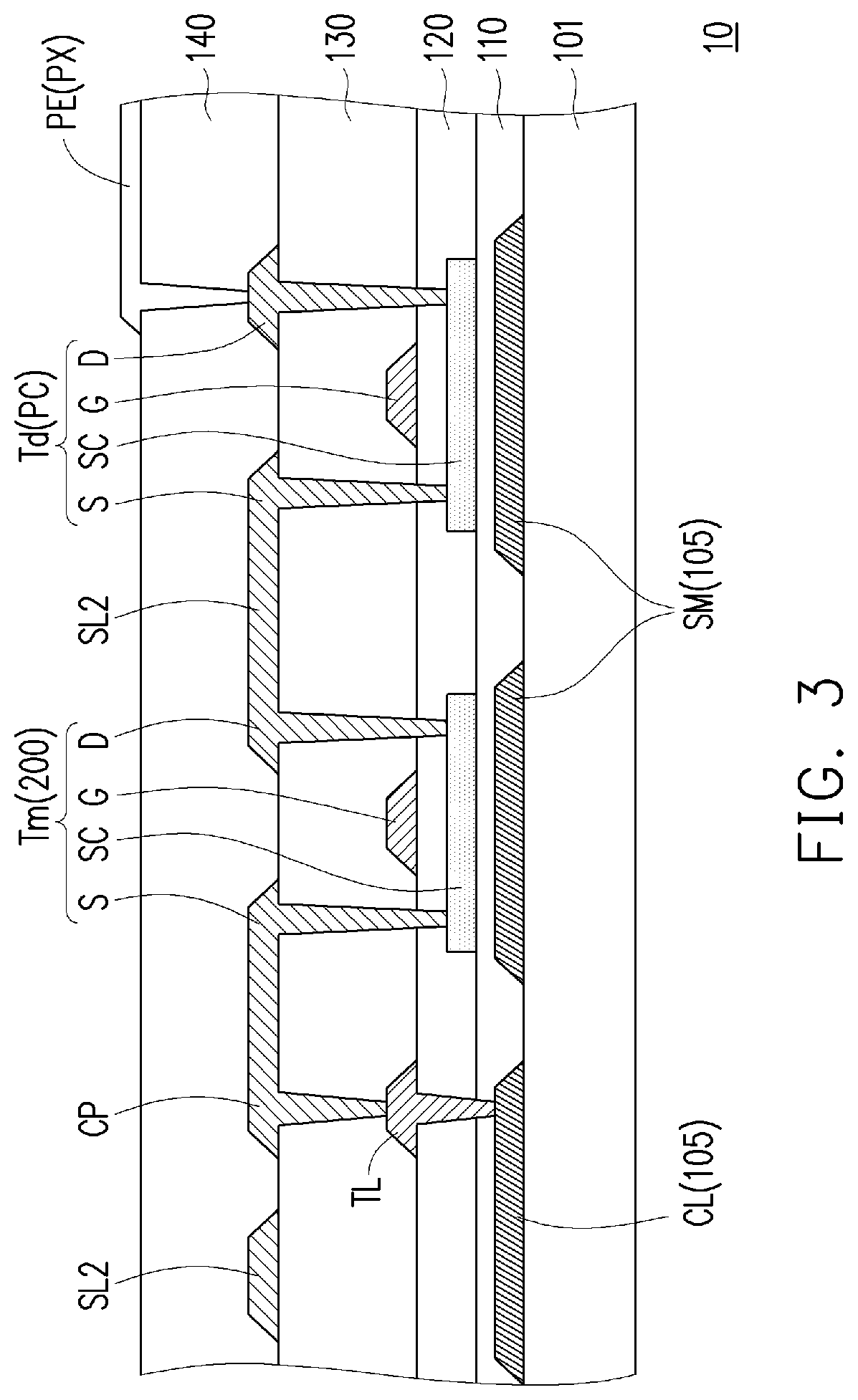
[0022]FIG. 1 is a schematic top view of a pixel array substrate according to the present application. FIG. 2 is an enlarged schematic view of a partial area of the pixel array substrate of FIG. 1. FIG. 3 is a partial cross-sectional view of the pixel array substrate of FIG. 2. In particular, for the sake of clarity, FIG. 1 omits the first signal line SL1 and the second signal line SL2 of FIG. 2, and FIG. 2 omits the buffer layer 110, the gate insulating layer 120, the interlayer insulating layer 130 and the planarization layer 140 of FIG. 3.
[0023]Referring to FIG. 1 and FIG. 2, the pixel array substrate 10 includes a substrate 101, a plurality of first signal lines SL1, a plurality of second signal lines SL2 and a plurality of pixels PX. The substrate 101 has a display area AA and a peripheral area PA disposed on one side of the display area AA. The first signal lines SL1 are arranged on the substrate 101, and define a plurality of row regions of the display area AA, such as the row...
second embodiment
[0039]FIG. 4 is a cross-sectional view of a pixel array substrate of the present application. Referring to FIG. 4, the main difference between the pixel array substrate 11 of the present embodiment and the pixel array substrate 10 of FIG. 3 lies in the arrangement of the connecting lines. In the present embodiment, the connection line CL1 and the connection line CL2A are belong to different film layers; for example, the connection line CL1 is formed in the first conductive layer 105, and the connection line CL2A is formed in the second conductive layer 155, and the first conductive layer 105 is located between the second conductive layer 155 and the substrate 101.
[0040]In detail, the planarization layer 140A of the present embodiment may be a stacked structure of the first planarization sublayer 141 and the second planarization sublayer 142, and the second conductive layer 155 is located between the first planarization sublayer 141 and the second planarization sublayer 142. The conn...
third embodiment
[0041]FIG. 5 is a schematic top view of a pixel array substrate according to the present application. FIG. 6 is an enlarged schematic view of a partial area of the pixel array substrate of FIG. 5. For the sake of clarity, FIG. 5 does not show the first signal line SL1 and second signal line SL2 of FIG. 6. Referring to FIG. 5 and FIG. 6, the main difference between the pixel array substrate 12 of the present embodiment and the pixel array substrate 10 of FIG. 1 lies in the arrangement of the multiplexers and the connection lines in the display area AA. In the present embodiment, multiple multiplexers 200 are respectively disposed in the row region RR4, the row region RR5 and the row region RR6 adjacent to the peripheral area PA, and any two adjacent multiplexers 200 are shifted from each other in the direction X. It is noted that by distributing these multiplexers 200 in different row regions, the design margin of multiplexer circuit (such as the number of control lines corresponding...
PUM
 Abstract
Description
Claims
Application Information
 - R&D
- Intellectual Property
- Life Sciences
- Materials
- Tech Scout
- Unparalleled Data Quality
- Higher Quality Content
- 60% Fewer Hallucinations
Browse by: Latest US Patents, China's latest patents, Technical Efficacy Thesaurus, Application Domain, Technology Topic, Popular Technical Reports.
© 2025 PatSnap. All rights reserved.Legal|Privacy policy|Modern Slavery Act Transparency Statement|Sitemap|About US| Contact US: help@patsnap.com