
NANO membrane, method of manufacturing NANO membrane, and apparatus for speaker and microphone using NANO membrane

a nano-layer and nano-technology, applied in the field of nano-layers, can solve the problems of inability to achieve flexibility with conventional bulk materials, impede the tight integration of personal electronic devices with other electronic devices, and exhibit extremely low bending stiffness of -based electronic devices, and achieve excellent transparency and conformal surface contact ability.

Pending Publication Date: 2020-10-22
UNIST (ULSAN NAT INST OF SCI & TECH)
View PDF9 Cites 1 Cited by
  • Summary
  • Abstract
  • Description
  • Claims
  • Application Information

AI Technical Summary

Benefits of technology

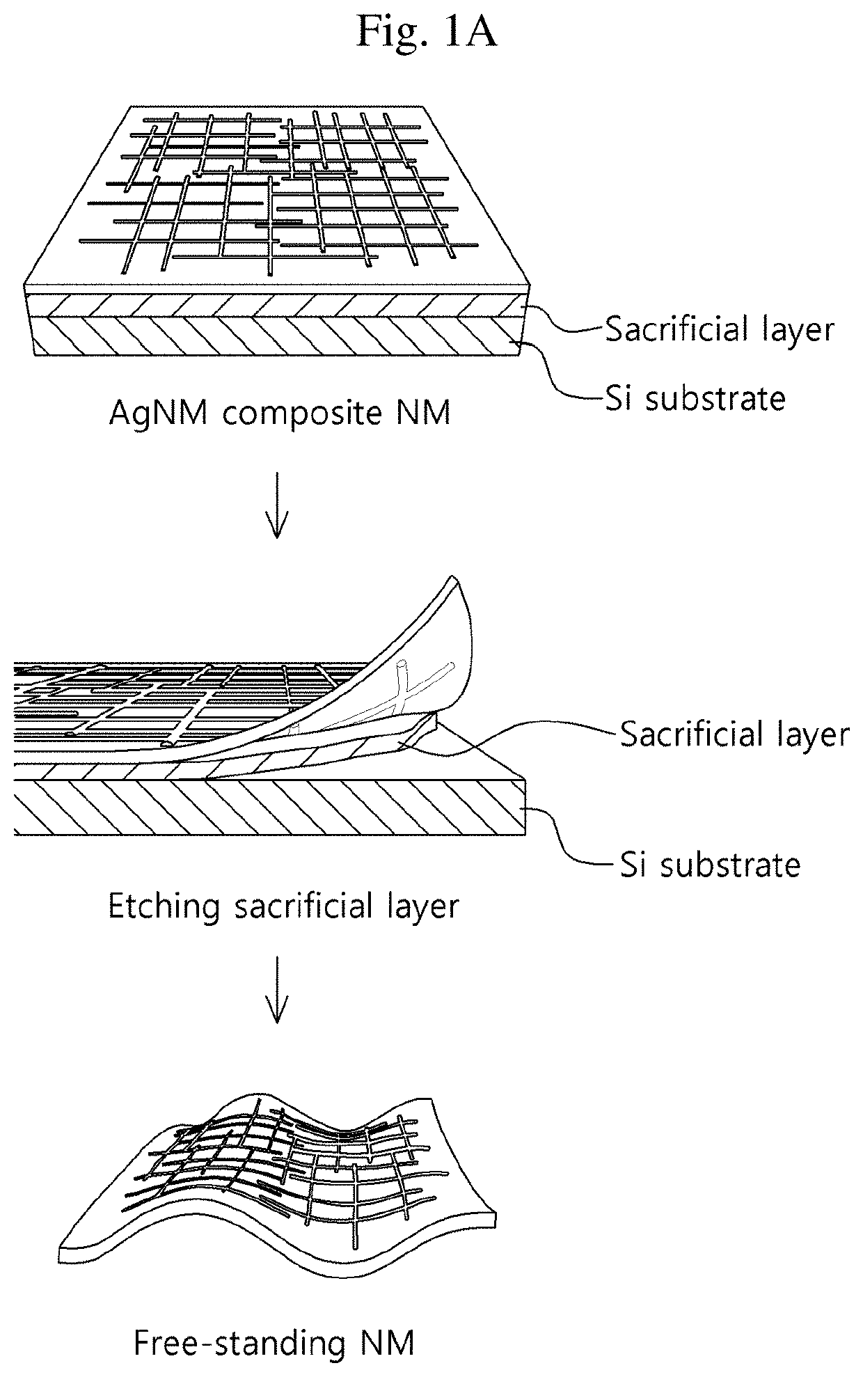
The patent describes a very thin and transparent conductive membrane made of silver nanowires that can be used to make products that can be in contact with the human body, a speaker, and a microphone. The membrane is easy to manufacture and is highly flexible and conformal, meaning it can be easily shaped to fit different devices. The technical effects of this invention are that it provides a discreet and comfortable material for use in various electronic devices.

Problems solved by technology

Nonetheless, such personal electronic devices still hinder tight integration with other electronic devices in the recent development of wearable devices.
This flexibility cannot be achieved with conventional bulk materials.
Although the nano membrane-based electronic devices exhibit extremely low bending stiffness to be capable of being in conformal contact with uneven surfaces, there is a problem in that mechanical properties of polymer nano membranes cause mechanical damage by external stress or deformation due to low fracture toughness.
Furthermore, in the past, there has been no attempt to develop a large-scale conductive silver nanowire composite nano membrane in an electronic device which can be attached to skin.

Method used


Image

  • NANO membrane, method of manufacturing NANO membrane, and apparatus for speaker and microphone using NANO membrane
  • NANO membrane, method of manufacturing NANO membrane, and apparatus for speaker and microphone using NANO membrane
  • NANO membrane, method of manufacturing NANO membrane, and apparatus for speaker and microphone using NANO membrane

Examples


Embodiment Construction

[0056]The terms a first, a second, and / or the like in this disclosure are used only for the purpose of distinguishing one component from another component. That is, components are not intended to be limited to these terms.

[0057]Components, features, and steps, which are referred to as “being included” in this disclosure, mean the presence of corresponding components, features, and steps and do not preclude the presence of one or more other components, features, steps, and equivalents thereof.

[0058]Unless the context clearly dictates otherwise, the singular form includes the plural form. That is, the components and the like referred to in this disclosure may mean the presence or addition of one or more other components or the like.

[0059]Unless defined otherwise, all terms including technical or scientific terms used herein have the same meaning as commonly understood by those skilled in the art (ordinary skilled persons) to which the present invention pertains.

[0060]That is, general ...


PUM

PropertyMeasurementUnit
heightaaaaaaaaaa
thicknessaaaaaaaaaa
optical transmittanceaaaaaaaaaa

Abstract

Disclosed herein is a nano membrane. The nano membrane includes an insulating layer having a thickness corresponding to a diameter of each of metal nanowires and configured to contain the metal nanowires therein, and the metal nanowires arranged to cross and having portions of side surfaces which protrude from one surface of the insulating layer.

Description

CROSS-REFERENCE TO RELATED APPLICATION[0001]This application is a divisional application of U.S. patent application Ser. No. 16 / 190,857 filed Nov. 14, 2018, which claims priority of Korean Patent Application Nos. 10-2017-0131633, filed on Oct. 11, 2017 and 10-2018-0111329, filed on Sep. 18, 2018, in the Korean Intellectual Property Office. The above-listed applications are incorporated herein by reference in their entirety.BACKGROUND1. Field of the Invention[0002]The present invention relates to a conductive nano membrane based on a metal nanowire composite, a method of manufacturing the nano membrane, and a speaker and a microphone using the nano membrane.2. Discussion of Related Art[0003]With the rapid growth of “Internet of Things (IoT),” which interconnects humans and machines, personal electronic devices have evolved into smart, portable, and miniaturized devices. Nonetheless, such personal electronic devices still hinder tight integration with other electronic devices in the r...

Claims


Application Information

Patent Timeline
Patent Type & Authority Applications(United States)
IPC IPC(8): H04R7/06B29C41/20H04R29/00H04R31/00H04R1/22H04R7/10
CPCH04R7/06H04R31/003H04R29/001H04R7/10B29L2031/755H04R1/22H04R29/004H04R2307/027B29C41/20B29K2705/00H04R2307/025H04R19/00H04R2201/003B29C66/03C08J7/02C23C26/00
Inventor KO, HYUNHYUBKANG, SAEWONCHO, SEUNGSE
Owner UNIST (ULSAN NAT INST OF SCI & TECH)
Learn More