
Matching circuit and communication device

Active Publication Date: 2020-07-16
MURATA MFG CO LTD
View PDF0 Cites 1 Cited by
  • Summary
  • Abstract
  • Description
  • Claims
  • Application Information

AI Technical Summary

Benefits of technology

The present invention provides matching circuits and communication devices that have low loss, can match impedance over a wide range of frequencies, and also have a filter function. These circuits can help improve the quality and efficiency of communication devices.

Problems solved by technology

Further, since the number of elements necessary for impedance matching is large, there is a tendency that a loss is large.
Since the filter is configured with an LC circuit, losses caused by an inductor and a capacitor inevitably increase by providing the filter.
In the high-frequency circuit that requires the impedance matching circuit and the filter, an increase in loss due to the provision of the filter is not limited to a circuit provided between an output portion of the power amplifier and the antenna, but is common among high-frequency circuits each of which includes an impedance matching circuit and a filter.

Method used


Image

  • Matching circuit and communication device
  • Matching circuit and communication device
  • Matching circuit and communication device

Examples


first preferred embodiment

[0053]A first preferred embodiment of the present invention is an example of an impedance matching circuit having low pass filter characteristics.

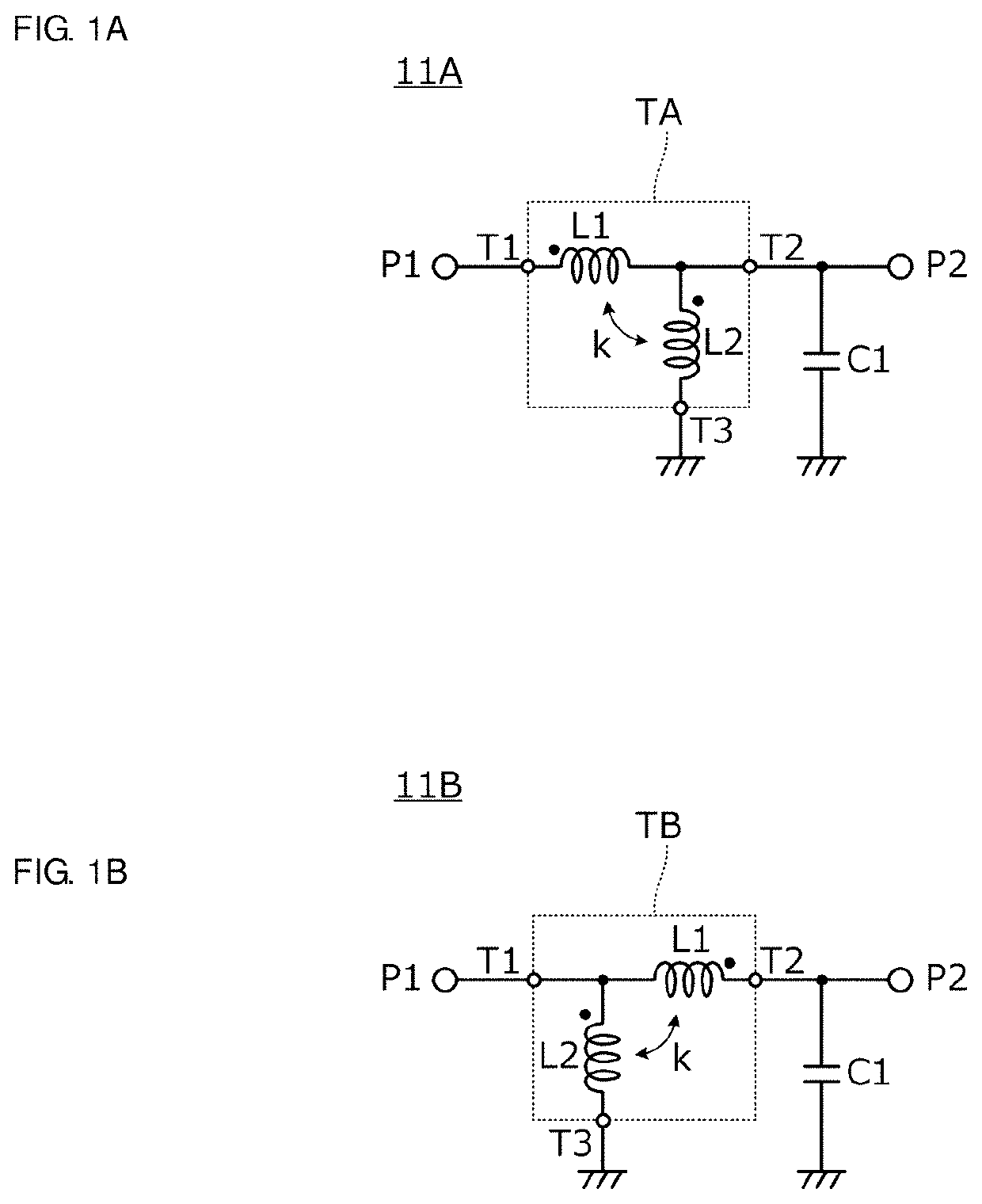
[0054]FIG. 1A is a circuit diagram of the matching circuit 11A according to the first preferred embodiment, and FIG. 1B is a circuit diagram of the matching circuit 11B according to the first preferred embodiment. The matching circuits 11A and 11B have a function of matching impedance between the first port P1 side impedance and the second port P2 side impedance, and a low pass filter function. The matching circuit 11A includes an autotransformer TA and a first capacitor C1. The matching circuit 11B includes the autotransformer TB and the first capacitor C1.

[0055]Each of the autotransformers TA and TB includes a first terminal T1 coupled to the first port P1, a second terminal T2 coupled to the second port P2, and a common terminal T3 coupled to a reference potential (ground).

[0056]The autotransformer TA of the matching circuit 11A include...

second preferred embodiment

[0081]A second preferred embodiment of the present invention is an example of an impedance matching circuit having high pass filter characteristics.

[0082]FIG. 6A is a circuit diagram of the matching circuit 12A according to the second preferred embodiment, and FIG. 6B is a circuit diagram of the matching circuit 12B according to the second preferred embodiment. The matching circuits 12A and 12B have a function of matching impedance between the first port P1 side impedance and the second port P2 side impedance, and a high pass filter function. The matching circuit 12A includes the autotransformer TA and a second capacitor C2. The matching circuit 12B includes the autotransformer TB and the second capacitor C2.

[0083]The configurations of the autotransformers TA and TB are as described in the first preferred embodiment.

[0084]In the matching circuits 12A and 12B, the second capacitor C2 is coupled in series between the first terminal T1 and the first port P1.

[0085]All of FIGS. 7A to 7C ...

third preferred embodiment

[0092]A third preferred embodiment of the present invention is an example of an impedance matching circuit having band pass filter characteristics.

[0093]FIG. 10A is a circuit diagram of the matching circuit 13A according to the third preferred embodiment, and FIG. 10B is an equivalent circuit diagram of the matching circuit 13A. The matching circuit 13A has a function of matching impedance between the first port P1 side impedance and the second port P2 side impedance, and a band pass filter function. The matching circuit 13A includes the autotransformer TA, the first capacitor C1, and the second capacitor C2.

[0094]The configuration of the autotransformer TA described above is as described in the first preferred embodiment.

[0095]In the matching circuit 13A, the first capacitor C1 is coupled in shunt between the second terminal T2 and the ground, and the second capacitor C2 is coupled in series between the first terminal T1 and the first port P1.

[0096]In FIG. 10B, the low pass filter ...


PUM


Abstract

A matching circuit includes first and second ports, an autotransformer, and first and second capacitors. The autotransformer includes a first terminal coupled to a first port, a second terminal coupled to a second port, and a common terminal coupled to a reference potential, and includes a series parasitic inductor and a parallel parasitic inductor. The first capacitor is coupled in shunt to the second terminal, and defines a low pass filter together with the series parasitic inductor. The second capacitor is coupled in series between the first port and the first terminal, and defines a high pass filter together with the parallel parasitic inductor.

Description

CROSS REFERENCE TO RELATED APPLICATIONS[0001]This application claims the benefit of priority to Japanese Patent Application No. 2017-204886 filed on Oct. 24, 2017 and is a Continuation Application of PCT Application No. PCT / JP2018 / 034140 filed on Sep. 14, 2018. The entire contents of each application are hereby incorporated herein by reference.BACKGROUND OF THE INVENTION1. Field of the Invention[0002]The present invention relates to a matching circuit in a high-frequency circuit such as an antenna matching circuit, and a communication device including the matching circuit.2. Description of the Related Art[0003]For example, a matching circuit for matching an output impedance of a power amplifier to impedance of an antenna is provided between the power amplifier and the antenna provided in a mobile phone terminal. Such a matching circuit is disclosed in, for example, Japanese Unexamined Patent Application Publication No. 2017-84898.[0004]FIG. 15A is a diagram illustrating an example o...

Claims


Application Information

Patent Timeline
IPC IPC(8): H03H7/38H03F1/56H03H7/09H03F3/21H04B1/04
CPCH03H7/09H03F1/565H04B2001/0408H04B1/04H03H7/38H03F2200/387H03F3/21H01Q1/50H03F3/245H03F3/19H03F2200/391H03F2200/541H04B1/0458
Inventor AKIYAMA, HISASHI
Owner MURATA MFG CO LTD
Learn More