Panel device and mamufacturing method thereof
a technology of display device and screen, which is applied in the field of display devices, can solve the problems of narrow frame display, inability to realize full screen display, and inability to reduce so as to increase the screen ratio of the display device and reduce the width of the frame. , the effect of narrow frame display
- Summary
- Abstract
- Description
- Claims
- Application Information
AI Technical Summary
Benefits of technology
Problems solved by technology
Method used
Image
Examples
first embodiment
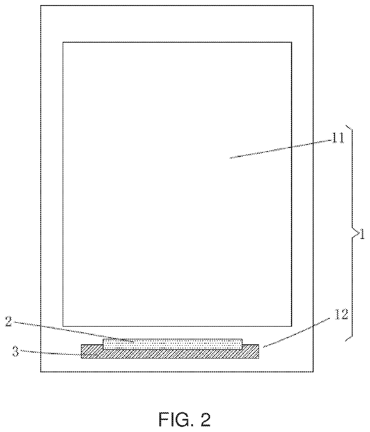
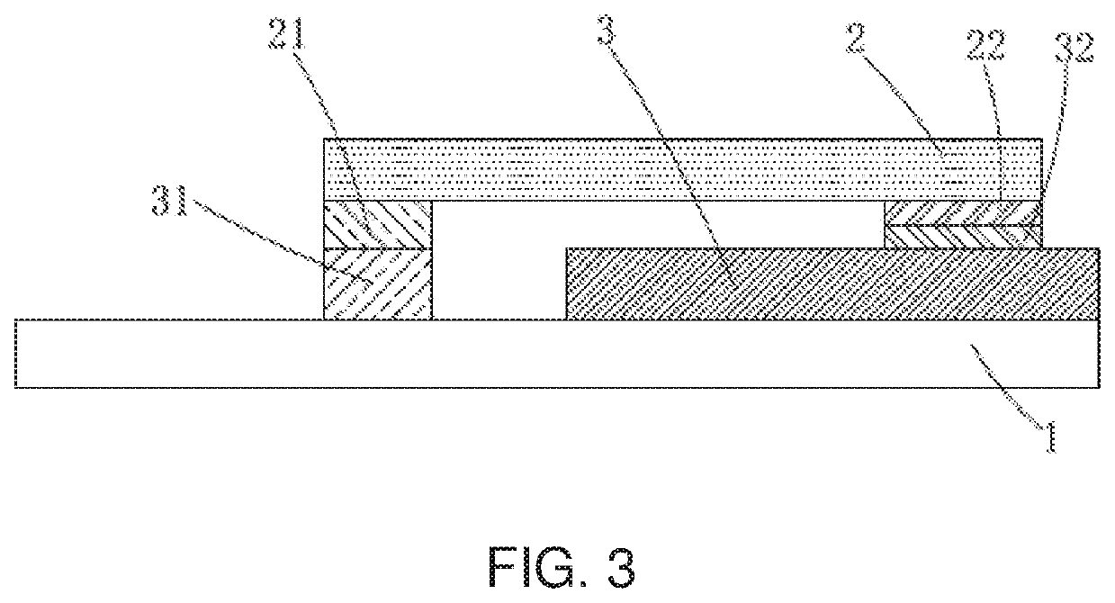
[0049]Specifically, as shown in FIGS. 2 and 3, in the present invention, a plurality of first pins 31 are disposed at intervals in the connecting area 12. A plurality of second pins 32 are disposed at intervals on a side surface of the flexible circuit board 3 away from the display panel 1. A plurality of output pins 21 are disposed on the driving chip 2 corresponding to the first pins 31 respectively, and a plurality of input pins 22 are disposed on the driving chip 2 corresponding to the second pins respectively 32. The driving chip 2 partially overlaps the flexible circuit board 3, each output pins 21 is bound to one of the first pins 31, and each input pins 22 is bound to one of the second pins 32.
[0050]Further, in the first embodiment of the present invention, the electrical connection between the flexible circuit board 3 and the driving chip 2 is realized through connecting the second pin 32 and the input pin 22, thereby transmitting an input signal to the driving chip 2 throu...
second embodiment
[0052]Specifically, as shown in FIG. 4 and FIG. 5, in the present invention, a plurality of first pins 31 are disposed at intervals in the connecting area 12. A plurality of second pins 32 are disposed at intervals on a side surface of the flexible circuit board 3 away from the display panel 1. A plurality of connection vias 33 are further formed on the flexible circuit board 3, and the connection vias 33 correspond to the first pins 31 respectively. Each of the connection vias 33 passes through the flexible circuit board 3 and correspondingly exposes one of the first pins 31. Each of the connection vias 33 is disposed within a connection pin 34, and an end of the connection pin 34 is bound to the first pin 31 corresponding to the connection vias 33. A plurality of output pins 21 are disposed on the driving chip 2 corresponding to the connection pins 34 respectively, and a plurality of input pins 22 are disposed on the driving chip 2 corresponding to the second pins 32 respectively....
PUM
 Abstract
Description
Claims
Application Information
 - R&D
- Intellectual Property
- Life Sciences
- Materials
- Tech Scout
- Unparalleled Data Quality
- Higher Quality Content
- 60% Fewer Hallucinations
Browse by: Latest US Patents, China's latest patents, Technical Efficacy Thesaurus, Application Domain, Technology Topic, Popular Technical Reports.
© 2025 PatSnap. All rights reserved.Legal|Privacy policy|Modern Slavery Act Transparency Statement|Sitemap|About US| Contact US: help@patsnap.com


