Manufacturing method of liquid crystal display and liquid crystal display

a liquid crystal display and manufacturing method technology, applied in the field of display technology, can solve the problems of not allowing for a frameless display, reducing the frame width of the lcd panel, and not allowing for a narrow frame display or a frameless display, so as to reduce the frame width of the liquid crystal display panel, narrow frame display, and reduce the effect of the frame width

Active Publication Date: 2021-10-12
WUHAN CHINA STAR OPTOELECTRONICS TECH CO LTD
View PDF8 Cites 0 Cited by
  • Summary
  • Abstract
  • Description
  • Claims
  • Application Information

AI Technical Summary

Benefits of technology

[0027]The benefits of the present invention are: the present invention provides a manufacturing method of a liquid crystal display, and in the manufacturing method of the liquid crystal display, a transparent flexible film is formed on an array substrate, and then, connection pins are formed on the transparent flexible film, and then, a portion of the transparent flexible film formed with the connection pins is fixed on a side of the array substrate away from an opposite substrate by bending, which can reduce a frame width of a liquid crystal display panel to achieve a narrow frame display. Another objective of the present invention is to provide a liquid crystal display device, which can reduce a frame width of a liquid crystal display panel to achieve a narrow frame display.

Problems solved by technology

However, in the conventional liquid crystal display, the connection pins for COF bonding are disposed on the array substrate, and for this purpose, a bonding region which cannot be used for display must be reserved at the edge of the array substrate to make connection pins, which causes the frame of the LCD panel to be further reduced, and does not allow for a narrow frame display or a frameless display.

Method used


Image

  • Manufacturing method of liquid crystal display and liquid crystal display
  • Manufacturing method of liquid crystal display and liquid crystal display
  • Manufacturing method of liquid crystal display and liquid crystal display

Examples


Embodiment Construction

[0040]For better explaining the technical solution and the effect of the present invention, the present invention will be further described in detail with the accompanying drawings and the specific embodiments.

[0041]Please refer to FIG. 10. The present invention provides a manufacturing method of a liquid crystal display, comprising steps of:

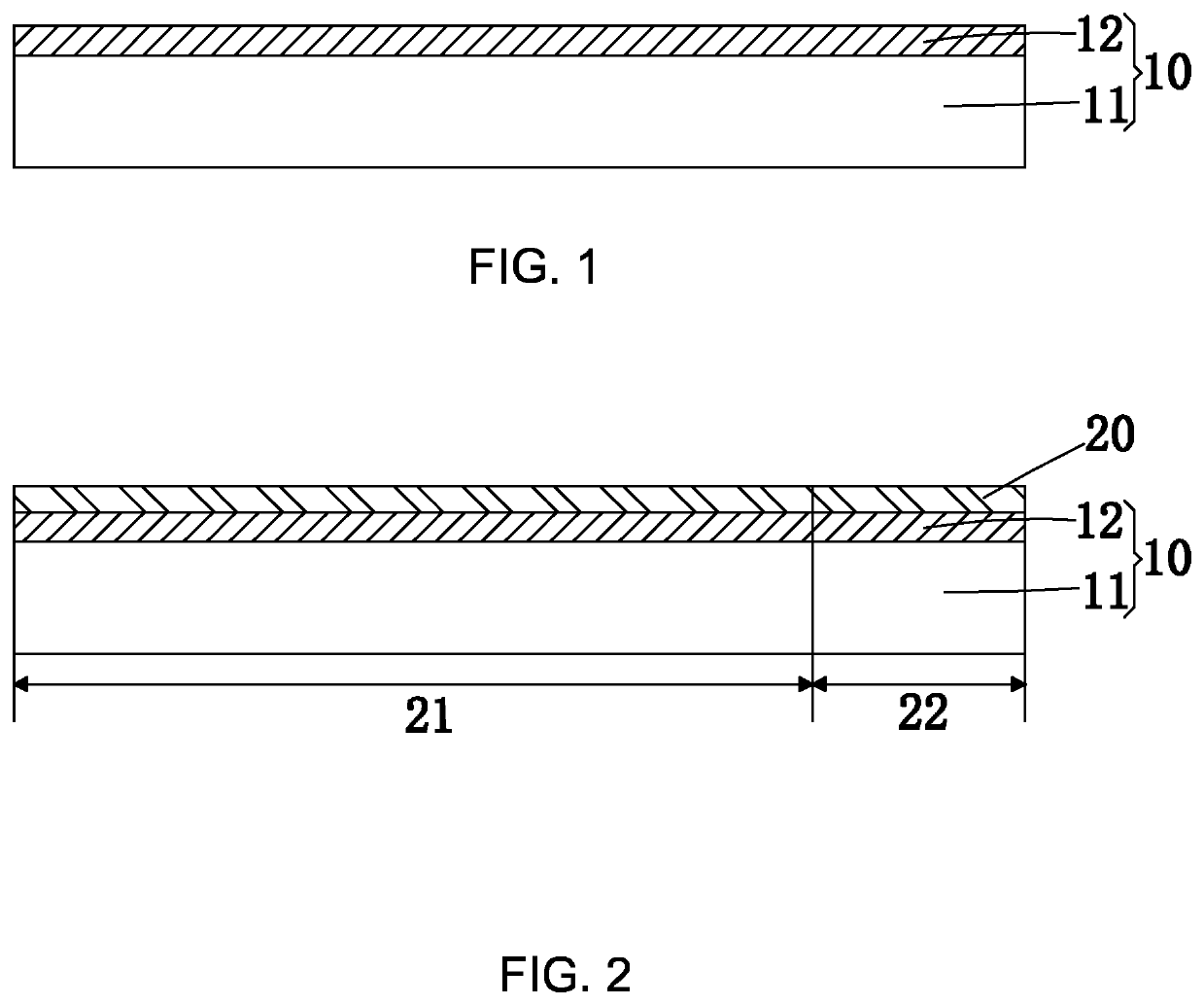
[0042]Step S1, referring to FIG. 1, providing an array substrate 10, wherein the array substrate 10 comprises a substrate 11 and a driving circuit 12 on the substrate 11.

[0043]Specifically, the substrate 11 is a rigid transparent substrate, and preferably is a glass substrate. The driving circuit includes: a thin film transistor (TFT) array, data lines and scan lines electrically connected to the TFT array, fan-out lines electrically connected to the scan lines and the data lines, and pixel electrodes electrically connected to the TFT array.

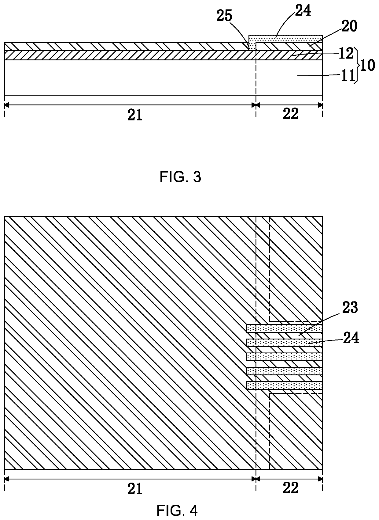
[0044]Step S2, referring to FIG. 2, forming a transparent flexible film 20 on the array substrate 10, wher...


PUM

PropertyMeasurementUnit
transparent flexibleaaaaaaaaaa
flexibleaaaaaaaaaa
voltagesaaaaaaaaaa

Abstract

Provided are a manufacturing method of a liquid crystal display and the liquid crystal display. In the manufacturing method of the liquid crystal display, a transparent flexible film is formed on an array substrate, and then, connection pins are formed on the transparent flexible film, and then, a portion of the transparent flexible film formed with the connection pins is fixed on a side of the array substrate away from an opposite substrate by bending, which can reduce a frame width of a liquid crystal display panel to achieve a narrow frame display.

Description

FIELD OF THE INVENTION[0001]The present invention relates to a display technology field, and more particularly to a manufacturing method of a liquid crystal display and the liquid crystal display.BACKGROUND OF THE INVENTION[0002]With the development of display technology, the flat panel device, such as Liquid Crystal Display (LCD) possesses advantages of high image quality, power saving, thin body and wide application scope. Thus, it has been widely applied in various consumer electrical products, such as mobile phone, television, personal digital assistant, digital camera, notebook, laptop, and becomes the major display device.[0003]The liquid crystal display panel of the prior art generally includes a CF (Color Filter) substrate, a TFT (Thin Film Transistor) array substrate, LC (Liquid Crystal) sandwiched between the CF substrate and TFT substrate and sealant. The working principle is that the light of backlight module is reflected to generate images by applying driving voltages t...

Claims


Application Information

Patent Timeline
Patent Type & Authority Patents(United States)
IPC IPC(8): G02F1/1345G02F1/1362
CPCG02F1/13452G02F1/13454G02F1/136227G02F1/13306G02F1/1333G02F1/133723H05K1/189H05K2201/10136
Inventor PAN, HAILONG
Owner WUHAN CHINA STAR OPTOELECTRONICS TECH CO LTD
Why Eureka
Try Eureka