Bifacial p-type perc solar cell and module, system, and preparation method thereof
a solar cell and p-type technology, applied in the field of solar cells, can solve the problems of complex process of manufacturing a bifacial n-type cell, high price of n-type silicon wafer, and limited photoelectric conversion efficiency, so as to simplify the laser process and printing process, and facilitate industrial production. scale-up, the effect of reducing the difficulty of debugging the printing devi
- Summary
- Abstract
- Description
- Claims
- Application Information
AI Technical Summary
Benefits of technology
Problems solved by technology
Method used
Image
Examples
embodiment 1
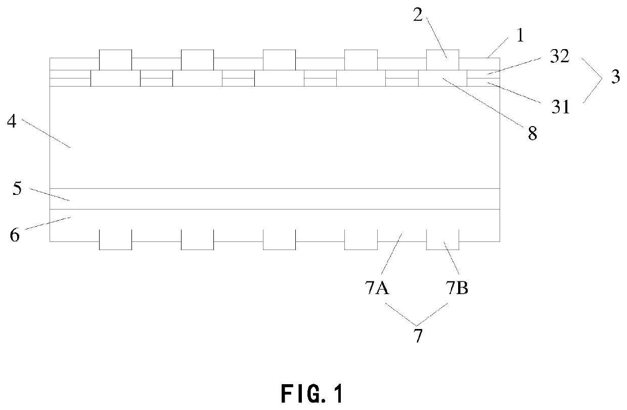
[0109](1) forming textured surfaces at a front surface and a rear surface of a silicon wafer, the silicon wafer being P-type silicon;
[0110](2) performing diffusion on the silicon wafer to form an N-type emitter;
[0111](3) removing phosphosilicate glass on the front surface and peripheral p-n junctions formed during the diffusion;
[0112](4) depositing an aluminum oxide (Al2O3) film on the rear surface of the silicon wafer;
[0113](5) depositing a silicon nitride film on the rear surface of the silicon wafer;
[0114](6) depositing a silicon nitride film on the front surface of the silicon wafer;
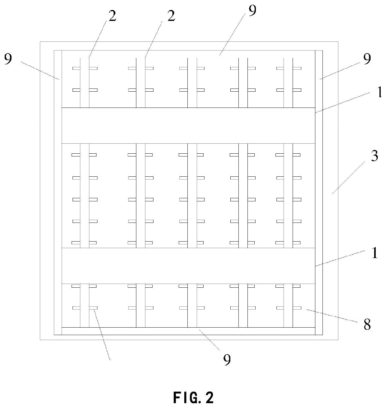
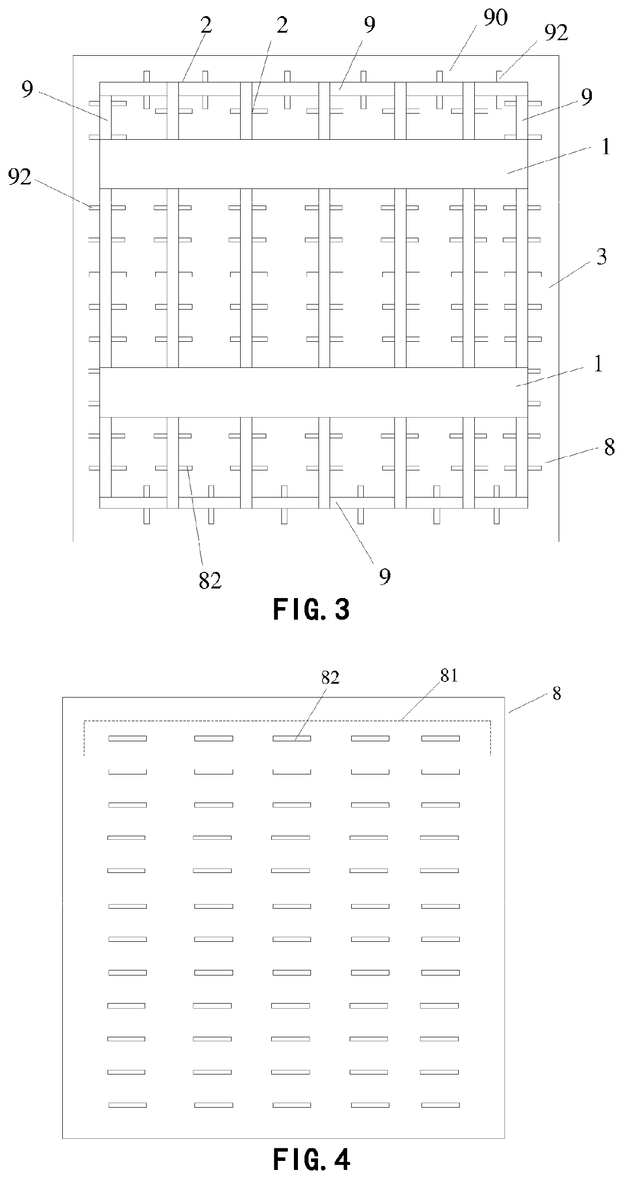
[0115](7) performing laser grooving in the rear surface of the silicon wafer to form a first laser grooving region, wherein the first laser grooving region includes a plurality of groups of first laser grooving units arranged horizontally, each group of the first laser grooving units includes one or more first laser grooving bodies arranged horizontally, wherein the first laser grooving body has a le...
embodiment 2
[0122](1) forming textured surfaces at a front surface and a rear surface of a silicon wafer, the silicon wafer being P-type silicon;
[0123](2) performing diffusion on the silicon wafer to form an N-type emitter;
[0124](3) removing phosphosilicate glass on the front surface and peripheral p-n junctions formed during the diffusion and polishing the rear surface of the silicon wafer;
[0125](4) depositing an aluminum oxide (Al2O3) film on the rear surface of the silicon wafer;
[0126](5) depositing a silicon nitride film on the rear surface of the silicon wafer;
[0127](6) depositing a silicon nitride film on the front surface of the silicon wafer;
[0128](7) performing laser grooving in the rear surface of the silicon wafer to form first and second laser grooving regions, wherein the first laser grooving region includes a plurality of groups of horizontally-arranged first laser grooving units, each group of the first laser grooving units includes one or more horizontally-arranged first laser g...
embodiment 3
[0136](1) forming textured surfaces at a front surface and a rear surface of a silicon wafer, the silicon wafer being P-type silicon;
[0137](2) performing diffusion on the silicon wafer to form an N-type emitter;
[0138](3) removing phosphosilicate glass on the front surface and peripheral p-n junctions formed during the diffusion;
[0139](4) depositing an aluminum oxide (Al2O3) film on the rear surface of the silicon wafer;
[0140](5) depositing a silicon nitride film on the rear surface of the silicon wafer;
[0141](6) depositing a silicon nitride film on the front surface of the silicon wafer;
[0142](7) performing laser grooving in the rear surface of the silicon wafer to form a first laser grooving region, wherein the first laser grooving region includes a plurality of groups of horizontally-arranged first laser grooving units, each group of the first laser grooving units includes one or more horizontally-arranged first laser grooving bodies, wherein the first laser grooving body has a le...
PUM
| Property | Measurement | Unit |
|---|---|---|
| width | aaaaa | aaaaa |
| length | aaaaa | aaaaa |
| width | aaaaa | aaaaa |
Abstract
Description
Claims
Application Information
 - R&D
- Intellectual Property
- Life Sciences
- Materials
- Tech Scout
- Unparalleled Data Quality
- Higher Quality Content
- 60% Fewer Hallucinations
Browse by: Latest US Patents, China's latest patents, Technical Efficacy Thesaurus, Application Domain, Technology Topic, Popular Technical Reports.
© 2025 PatSnap. All rights reserved.Legal|Privacy policy|Modern Slavery Act Transparency Statement|Sitemap|About US| Contact US: help@patsnap.com


