Flip-flop

a flip-flop and flip-flop technology, applied in the field of flip-flops, can solve the problems that the conventional master-slave flip-flop cannot meet the low power level, and the conventional master-slave flip-flop consumes power, so as to prevent unnecessary power consumption and low power

Active Publication Date: 2019-12-12
SAMSUNG ELECTRONICS CO LTD
View PDF0 Cites 1 Cited by
  • Summary
  • Abstract
  • Description
  • Claims
  • Application Information

AI Technical Summary

Benefits of technology

The flip-flop described in this patent operates with low power by preventing the internal nodes from being repeatedly charged and discharged in response to a clock signal while the input data is not changed. This is achieved by cross-connecting the internal nodes and charging them with inverted input data or the input data itself. This helps to prevent unnecessary power consumption and ensures the flip-flop operates efficiently.

Problems solved by technology

However, since a conventional master-slave flip-flop includes internal nodes that are repeatedly (e.g., alternately) charged and discharged in response to a clock signal, the conventional master-slave flip-flop consumes power even while input data is not changed.
Thus, the conventional master-slave flip-flop cannot satisfy the low power level that a recent mobile device of which an operating frequency is relatively high requires.

Method used


Image

  • Flip-flop
  • Flip-flop
  • Flip-flop

Examples


Embodiment Construction

[0031]Hereinafter, some example embodiments will be explained in detail with reference to the accompanying drawings.

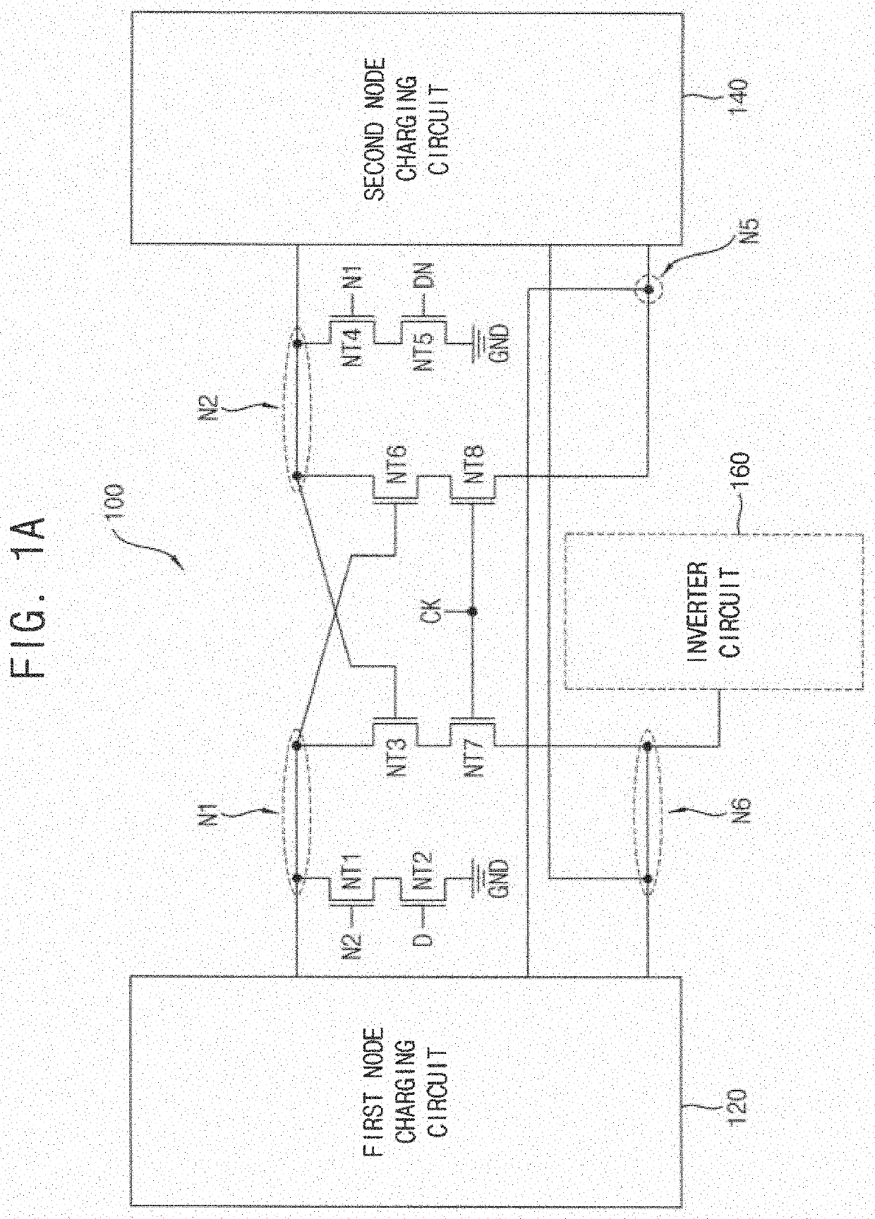
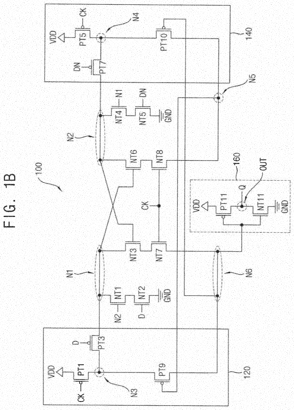
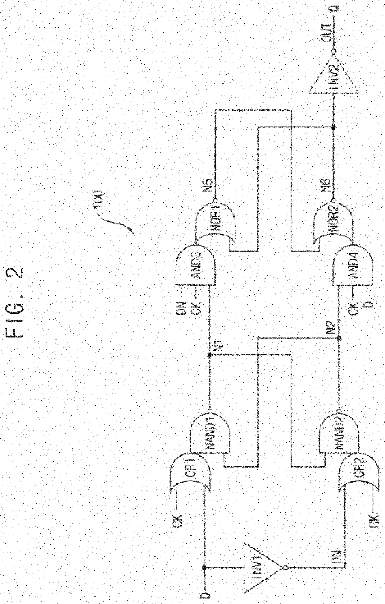
[0032]FIG. 1A is a circuit diagram illustrating a flip-flop according to some example embodiments. FIG. 1B is a detailed circuit diagram illustrating the flip-flop of FIG. 1A. FIG. 2 is a block diagram illustrating an example in which the flip-flop of FIG. 1B is implemented by logic elements. FIG. 3 is a timing diagram illustrating an example in which the flip-flop of FIG. 1B operates.

[0033]Referring to FIGS. 1A through 3, the flip-flop 100 may include a first node charging circuit 120, a second node charging circuit 140, and first through eighth n-channel metal oxide semiconductor (NMOS) transistors NT1 through NT8. In some example embodiments, the flip-flop 100 may further include an inverter circuit 160. Based on the above structure, the flip-flop 100 may latch input data D at rising edges of a clock signal CK and may output latched input data D as output data Q. In...


PUM


Abstract

A flip-flop includes a first node charging circuit configured to charge a first node with inverted input data generated by inverting input data, a second node charging circuit configured to charge a second node with the input data, and first through eighth NMOS transistors. The flip-flop is configured to latch the input data at rising edges of a clock signal and output latched input data as output data. The flip-flop includes an internal circuit configured to charge a sixth node with inverted input data generated by inverting the latched input data.

Description

CROSS-REFERENCE TO RELATED APPLICATION(S)[0001]This application is a continuation of U.S. patent application Ser. No. 15 / 669,072, filed on Aug. 4, 2017, which claims priority under 35 USC § 119 to Korean Patent Application No. 10-2016-0156812, filed on Nov. 23, 2016 in the Korean Intellectual Property Office (KIPO), the contents of each of which are incorporated herein in its entirety by reference.BACKGROUND1. Technical Field[0002]Example embodiments relate generally to a logic circuit. More particularly, some example embodiments relate to a flip-flop that latches input data at rising edges of a clock signal and outputs latched input data as output data.2. Description of the Related Art[0003]Recently, according to a mobile convergence trend, there is a rising interest on a low power technology for a mobile device (e.g., a smart phone, a smart pad, etc.). Generally, since the mobile device uses a limited power such as a battery, manufacturing (or, designing) the mobile device with lo...

Claims


Application Information

Patent Timeline
Patent Type & Authority Applications(United States)
IPC IPC(8): H03K3/012H03K3/3562H03K3/356
CPCH03K3/356182H03K3/35625H03K3/012H03K3/021H03K19/00346H03K3/3562H03K3/0372
Inventor HWANG, HYUN-CHULKIM, MIN-SULEE, DAE-SEONG
Owner SAMSUNG ELECTRONICS CO LTD
Why Eureka
Try Eureka