Semiconductor apparatus for power supply control and output voltage variable power supply apparatus
a technology of power supply control and circuit, applied in the direction of control system, dc motor speed/torque control, instruments, etc., can solve the problems of increasing electric power consumption, and difficult to make the circuit smaller
- Summary
- Abstract
- Description
- Claims
- Application Information
AI Technical Summary
Benefits of technology
Problems solved by technology
Method used
Image
Examples
first embodiment
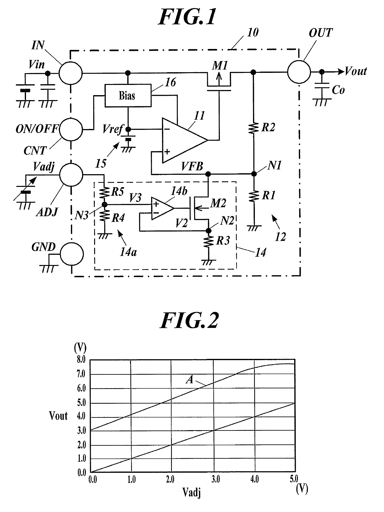
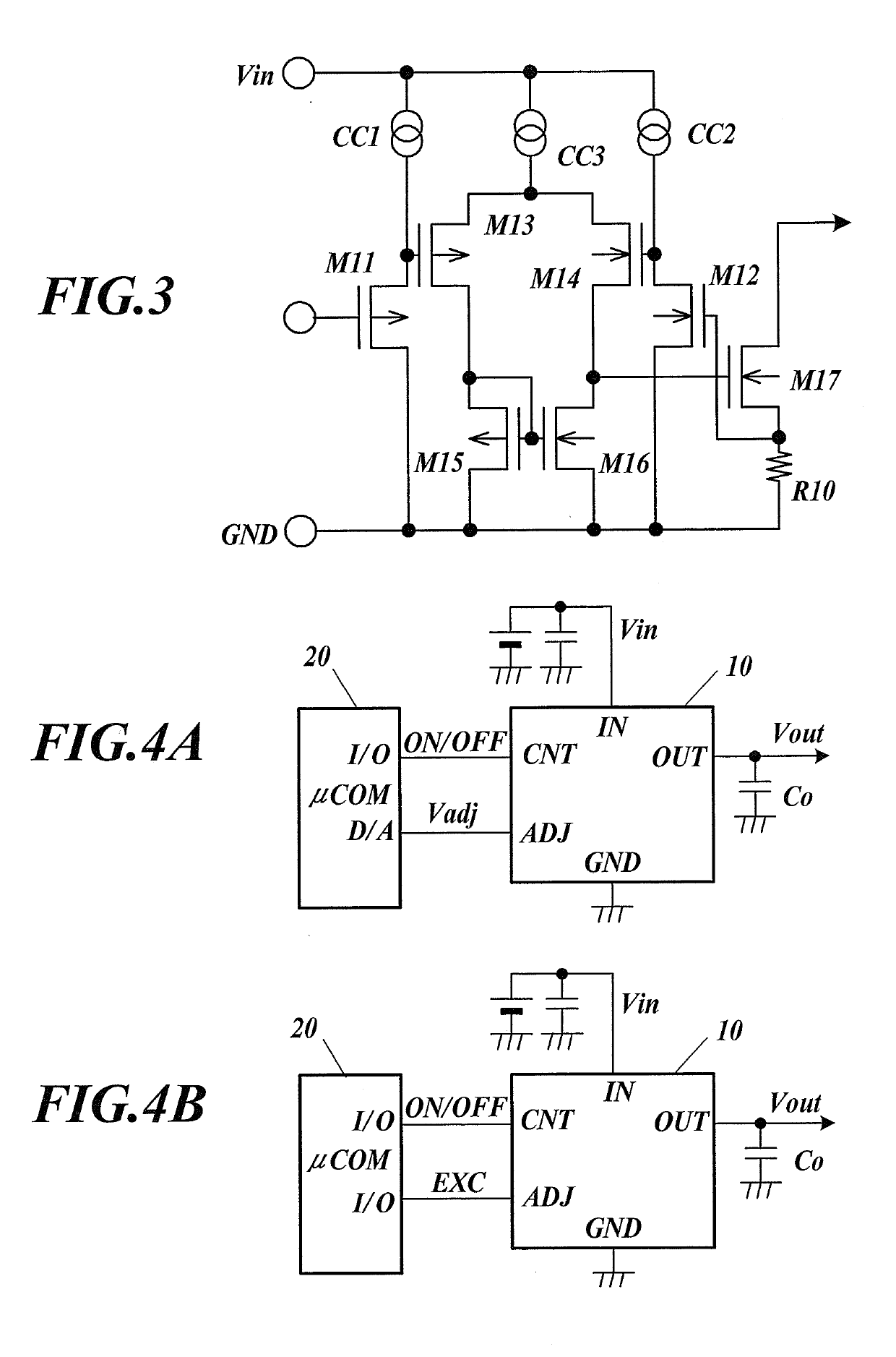
[0030]FIG. 1 shows a first embodiment of a series regulator as an output voltage variable power supply apparatus applying the present invention. In FIG. 1, the portion surrounded by a short and long dash line is formed as a semiconductor integrated circuit (regulator IC) 10 on a semiconductor chip such as single crystal silicon. The above functions as an output voltage variable power supply apparatus which outputs a stable DC voltage to a load such as a motor or LED lamp (not shown) by connecting a condenser Co to an output terminal OUT of the regulator IC 10.
[0031]As shown in FIG. 1, according to the output voltage variable power supply apparatus of the present embodiment, P-channel MOS transistor M1 to control the voltage (insulated gate electric field effect transistor) is connected between a voltage input terminal IN and an output terminal OUT on which input DC voltage yin of the regulator IC 10 is applied. Resistors R2 and R1 composing a pressure dividing circuit 12 which divid...
second embodiment
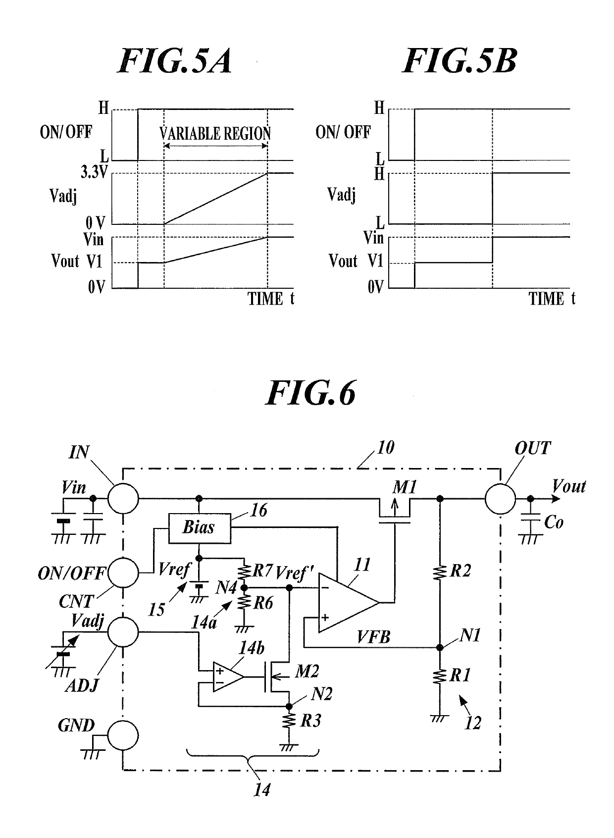
[0057]FIG. 7 shows a second embodiment of the regulator IC 10 including a series regulator as the output voltage variable power supply apparatus applying the present invention.
[0058]Instead of providing the voltage dividing circuit 14a of the output voltage changing circuit 14 in the first embodiment shown in FIG. 1, the output voltage variation power supply apparatus according to the present embodiment includes a first current mirror circuit 17a including transistors Tr1 and Tr2 connecting the base terminals of each other and a second current mirror circuit 17B including transistors Tr3 and Tr4 connecting the base terminals of each other as shown in FIG. 7.
[0059]The base terminal and the collector terminal of the transistors Tr1 and Tr3 are connected to function as the current-voltage conversion element. The converted voltage is applied to the transistors Tr2 and Tr4. With this, the electric current according to an emitter size ratio of the Tr1 and Tr2 and an emitter size ratio of ...
PUM
 Abstract
Description
Claims
Application Information
 - R&D
- Intellectual Property
- Life Sciences
- Materials
- Tech Scout
- Unparalleled Data Quality
- Higher Quality Content
- 60% Fewer Hallucinations
Browse by: Latest US Patents, China's latest patents, Technical Efficacy Thesaurus, Application Domain, Technology Topic, Popular Technical Reports.
© 2025 PatSnap. All rights reserved.Legal|Privacy policy|Modern Slavery Act Transparency Statement|Sitemap|About US| Contact US: help@patsnap.com


