
Method for connecting components of a microfluidic flow cell

a microfluidic flow cell and component technology, applied in the field of connecting components of microfluidic flow cells, can solve the problems high cost of materials, and achieve the effects of increasing functional complexity, low cost, and high cost of materials

Active Publication Date: 2019-09-12
THINXXS MICROTECHNOLOGY AG
View PDF5 Cites 0 Cited by
  • Summary
  • Abstract
  • Description
  • Claims
  • Application Information

AI Technical Summary

Benefits of technology

[0006]It is known from WO 2012 / 004296 A1 that microcomponents of glass or silicon can be integrated into carrier structures of plastic by means of an adhesive material which can be cured by UV radiation, for example. The disadvantage here is that there is now a third material present, i.e., not only the plastic material of the carrier structure and the material of the microcomponent integrated into it but also the adhesive material, which can then come into direct contact with the fluids to be tested. This can result in faulty measurements. Nor is it possible to exclude the possibility of toxic effects on the biological sample material. Another disadvantage is that such adhesive materials have a comparatively high viscosity and low wettability, which leads to the result that an adhesive of this type will not fill up an assembly gap by itself; that is, there will be no capillary action. Considerable effort is therefore required to transport the adhesive into such an assembly gap. The curing of adhesive materials filling assembly gaps by means of UV radiation, for example, is time-consuming, and the fabrication results are often unreliable. The low wettability requires wide gaps, and this in turn impairs the accuracy with which the microcomponents can be positioned in the carrier structure. The UV radiation used for curing can have disadvantageous effects on functionalized microcomponents, and in particular it can destroy antibodies immobilized on the functionalized surface of a microcomponent. The same is true for the use of heat to cure adhesives.
[0007]The invention pertains to a method for connecting components of a microfluidic flow cell, especially for integrating microcomponents into a carrier structure of the flow cell. The invention also pertains to a flow cell produced by the method.
[0008]The primary area of application for the method under consideration is the production of flow cells such as those used, for example, in medical analysis and diagnostics, in biochemistry, and in molecular biology as well as in drug development; these flow cells comprise a carrier structure of plastic, into which functional components, especially sensors of silicon, glass, or metal, are integrated. Flow cells of this type are undergoing a process of progressive miniaturization and increasing functional complexity, with the result that such flow cells are now being called “labs on a chip”.
[0009]In the production of these miniaturized flow cells, functional structures with dimensions ranging from a few 10 μm to a few 100 μm must be produced. In these functional structures, surface properties play a dominant role with respect to, for example, the capillary filling of channels and sample chambers. In addition, assembly techniques are required which make it possible to seal off microchambers and channels in a liquid-tight and pressure-proof manner and especially to form closed microfluidic networks. It takes a great deal of effort to produce such flow cells at low cost in large numbers so that they can be used in the field of medical diagnostics, for example.
[0010]Methods borrowed from semiconductor technology are used in the production of these flow cells, especially for the microstructuring of glass or silicon substrates. Especially in the production of complex flow cells, the cost of materials can be very high. A second production technique which is used is based on replication methods, e.g., injection-molding or stamping. It is possible by this means to produce substrates of plastic such as PMMA, PC, PP, or COC at low cost, the surfaces of which can then be modified and / or functionalized by plasma coating or wet-chemical methods. Adhesive methods can be used to mount substrates of this kind, but laser welding methods are also possible. The aspect ratios realizable by this latter method, however are much lower than in the methods of semiconductor technology, which is a disadvantage.
[0011]It is known from WO 2012 / 004296 A1 that microcomponents of glass or silicon can be integrated into carrier structures of plastic by means of an adhesive material which can be cured by UV radiation, for example. The disadvantage here is that there is now a third material present, i.e., not only the plastic material of the carrier structure and the material of the microcomponent integrated into it but also the adhesive material, which can then come into direct contact with the fluids to be tested. This can result in faulty measurements. Nor is it possible to exclude the possibility of toxic effects on the biological sample material. Another disadvantage is that such adhesive materials have a comparatively high viscosity and low wettability, which leads to the result that an adhesive of this type will not fill up an assembly gap by itself; that is, there will be no capillary action. Considerable effort is therefore required to transport the adhesive into such an assembly gap. The curing of adhesive materials filling assembly gaps by means of UV radiation, for example, is time-consuming, and the fabrication results are often unreliable. The low wettability requires wide gaps, and this in turn impairs the accuracy with which the microcomponents can be positioned in the carrier structure. The UV radiation used for curing can have disadvantageous effects on functionalized microcomponents, and in particular it can destroy antibodies immobilized on the functionalized surface of a microcomponent. The same is true for the use of heat to cure adhesives.

Problems solved by technology

Flow cells of this type are undergoing a process of progressive miniaturization and increasing functional complexity, with the result that such flow cells are now being called “labs on a chip”.
Especially in the production of complex flow cells, the cost of materials can be very high.
The aspect ratios realizable by this latter method, however are much lower than in the methods of semiconductor technology, which is a disadvantage.

Method used


Image

  • Method for connecting components of a microfluidic flow cell
  • Method for connecting components of a microfluidic flow cell
  • Method for connecting components of a microfluidic flow cell

Examples


Embodiment Construction

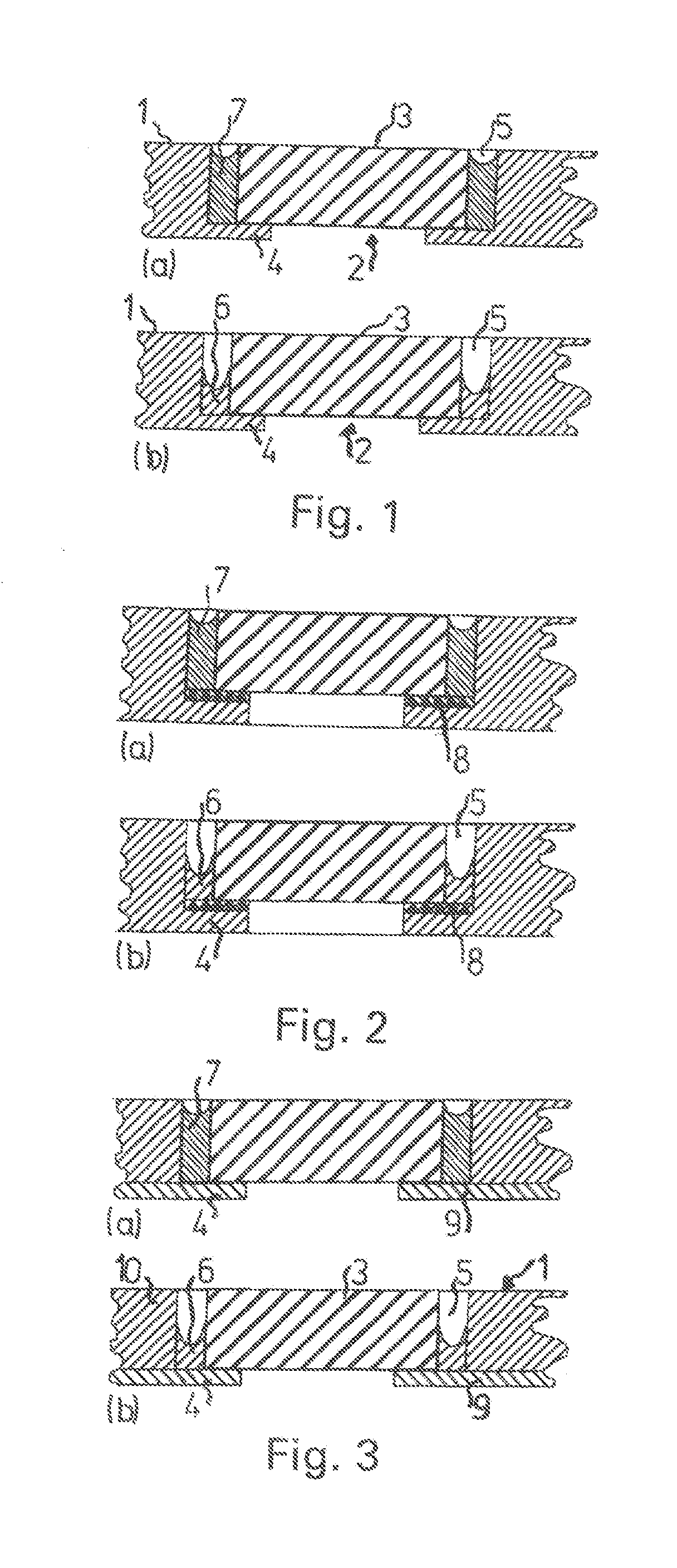
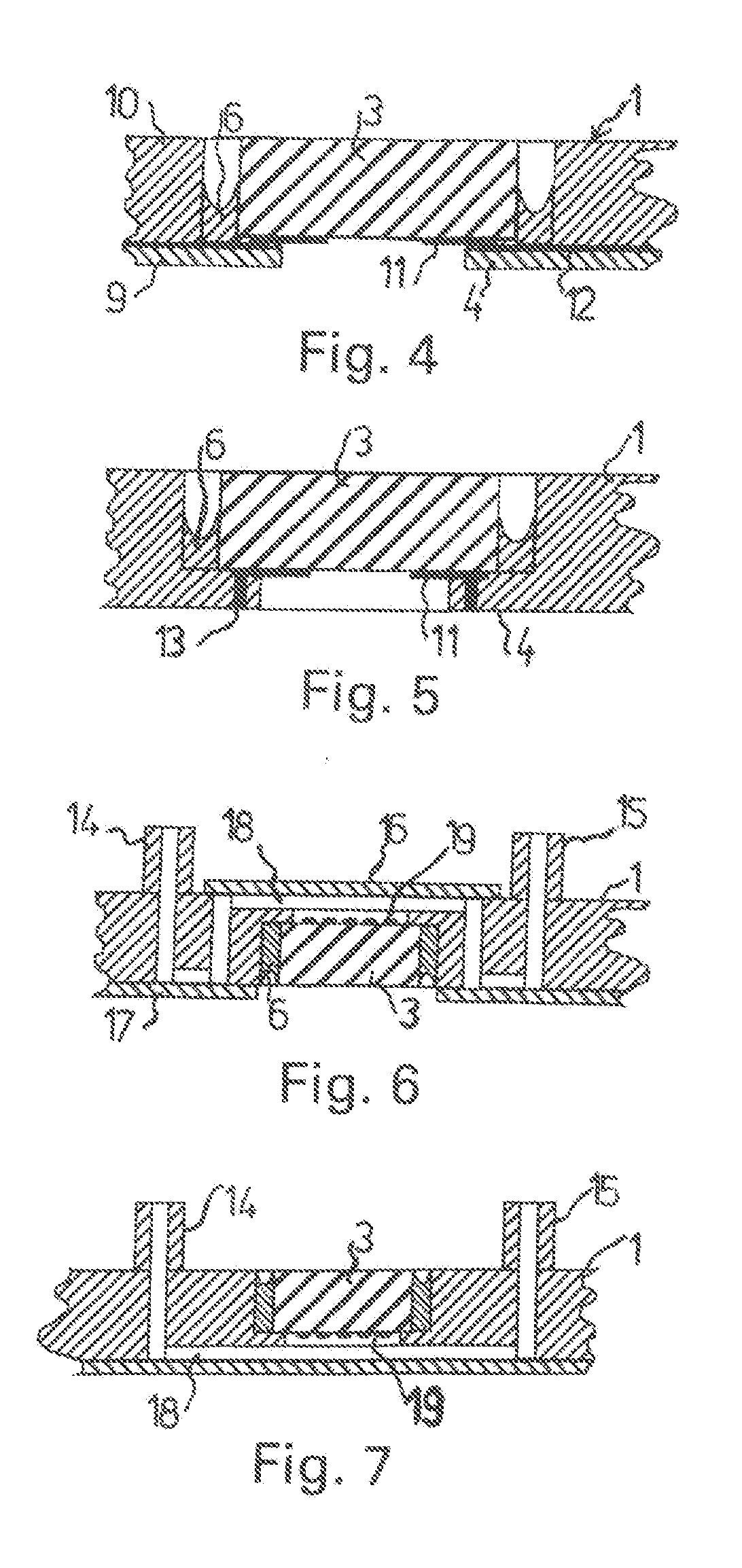
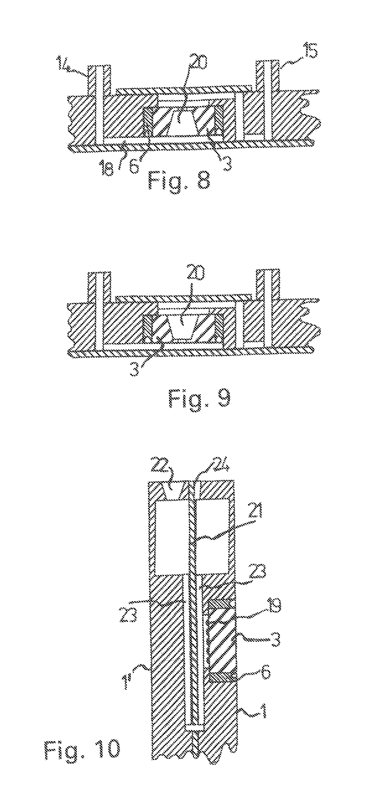
[0038]A microfluidic flow cell as shown partially in FIG. 1 comprises a plate-shaped carrier structure 1, which consists preferably of an amorphous plastic such as PMMA, PC, PS, COC, or COP.

[0039]A microcomponent 3—in the example shown, a component with the basic form of a circular disk or a square plate—is arranged in a pocket 2 of the carrier structure 1. The microcomponent is preferably made of silicon, but it can also be formed out of metal, ceramic, plastic, or glass with a surface which can be functionalized in various ways.

[0040]The microcomponent 3 rests on a ring-shaped shoulder 4 of the pocket 2; except for this shoulder, the pocket passes straight through the entire thickness of the carrier structure 1. An annular gap 5, formed between the carrier structure 1 and the microcomponent 3, is open on one axial side, whereas, on the other axial side, it is closed off by the ring-shaped shoulder 4 of the carrier structure 1. The width 3 of the annular gap 5 is typically in the r...


PUM

PropertyMeasurementUnit
contact anglesaaaaaaaaaa
thicknessaaaaaaaaaa
thicknessaaaaaaaaaa

Abstract

A flow cell and a method for connecting components of a microfluidic flow cell, in particular for integrating component parts into a carrier structure of the flow cell, in which a gap is formed between the components to be connected. The gap is filled with a solvent. The material of at least one component bordering the gap dissolves in the solvent and the material completely fills the width of the gap and partially fills the height thereof after evaporation of the solvent.

Description

CROSS-REFERENCE TO RELATED APPLICATIONS[0001]The present application is a Divisional Application of U.S. patent application Ser. No. 14 / 652,316, filed Jun. 15, 2015, which is a 371 of International Application PCT / DE2013 / 100408 filed on Dec. 5, 2013 which claims the benefit of priority from German Patent Application No. 10 2012 112 306.3 filed Dec. 14, 2012, the contents of each of which are incorporated herein by reference.BACKGROUND OF THE INVENTION[0002]The invention pertains to a method for connecting components of a microfluidic flow cell, especially for integrating microcomponents into a carrier structure of the flow cell. The invention also pertains to a flow cell produced by the method.[0003]The primary area of application for the method under consideration is the production of flow cells such as those used, for example, in medical analysis and diagnostics, in biochemistry, and in molecular biology as well as in drug development; these flow cells comprise a carrier structure...

Claims


Application Information

Patent Timeline
Patent Type & Authority Applications(United States)
IPC IPC(8): B01L3/00B29C65/00B29C65/48B29C65/54
CPCB29L2022/00B29C65/4895B29C65/54B29C66/1222B01L3/502707B01L2200/027B29C66/73771B29C66/61B01L2300/0816B01L2300/0636B29C66/7392B29C66/5346B01L2300/0877B01L2300/0645B01L2200/12B01L2300/12B29C66/47B29C66/1224B01L2200/0689B29C66/71B29L2031/756B29K2033/12B29K2069/00B29K2025/06B29K2023/38
Inventor WEBER, LUTZ
Owner THINXXS MICROTECHNOLOGY AG
Learn More