
Display device

a display device and display technology, applied in the field of liquid crystal display, can solve the problems of increasing the distance between the fingerprint recognition module and the human finger, reducing the performance of the fingerprint recognition module to identify and sense the human finger, and increasing the manufacturing process difficulty of the front glass cover. , to achieve the effect of improving the screen ratio of the display device and improving the accuracy of fingerprint recognition

Inactive Publication Date: 2019-08-08
WUHAN CHINA STAR OPTOELECTRONICS SEMICON DISPLAY TECH CO LTD
View PDF18 Cites 6 Cited by
  • Summary
  • Abstract
  • Description
  • Claims
  • Application Information

AI Technical Summary

Benefits of technology

The present invention provides a display device that can improve its screen ratio and fingerprint recognition accuracy. This is achieved by arranging a fingerprint recognition module in an opening on the back surface of the display panel, reducing the distance between the fingerprint recognition module and the display panel. The fingerprint recognition module can be located at any position in middle range of the display panel, improving both the screen ratio and fingerprint recognition accuracy.

Problems solved by technology

Prior art display devices increase thickness of a front glass cover to protect internal elements, which increases not only distance between the fingerprint recognition module and a human finger, but also greatly reduces performance of the fingerprint recognition module to identify and sense the human finger.
But this affects integrity of the front glass cover of the display device, and also increase manufacturing process difficulty of the front glass cover, and thereby increasing manufacturing cost.
In addition, the independent fingerprint recognition module is located on the upper and / or lower edges of the display device, which usually occupies a lot of space of the display area of the display device, thereby reducing screen ratio of the display area.

Method used


Image

  • Display device
  • Display device
  • Display device

Examples


Embodiment Construction

[0032]In order to make objects, technical details and advantages of the embodiments of the invention apparent, the technical solutions of the embodiment will be described in a clearly and fully understandable way in connection with the drawings related to the embodiments of the invention. It is obvious that the described embodiments are just a part but not all of the embodiments of the invention. Based on the described embodiments herein, those skilled in the art can obtain other embodiment(s), without any inventive work, which should be within the scope of the invention.

[0033]Throughout this specification and in the drawings like parts will be referred to by the same reference numerals.

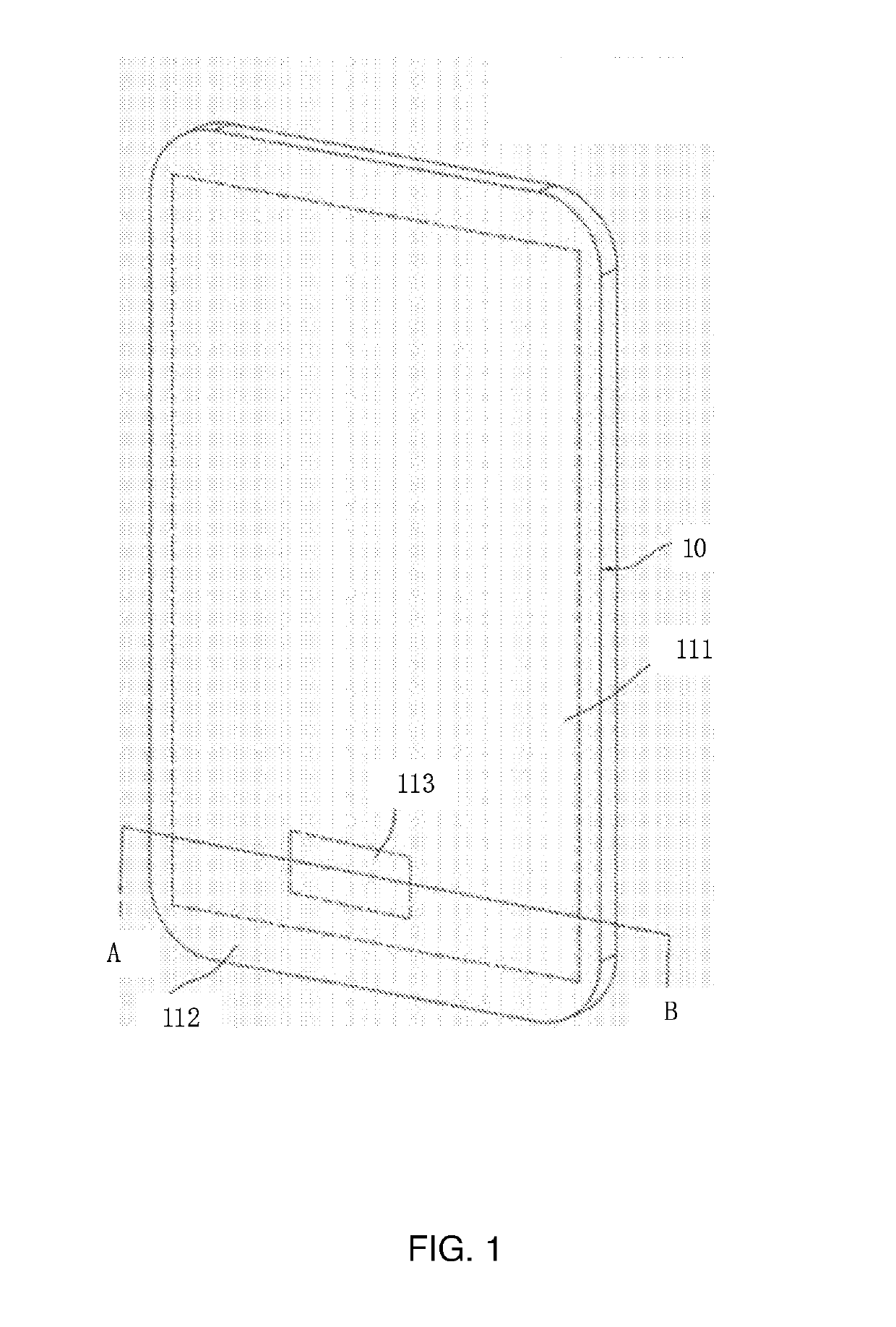
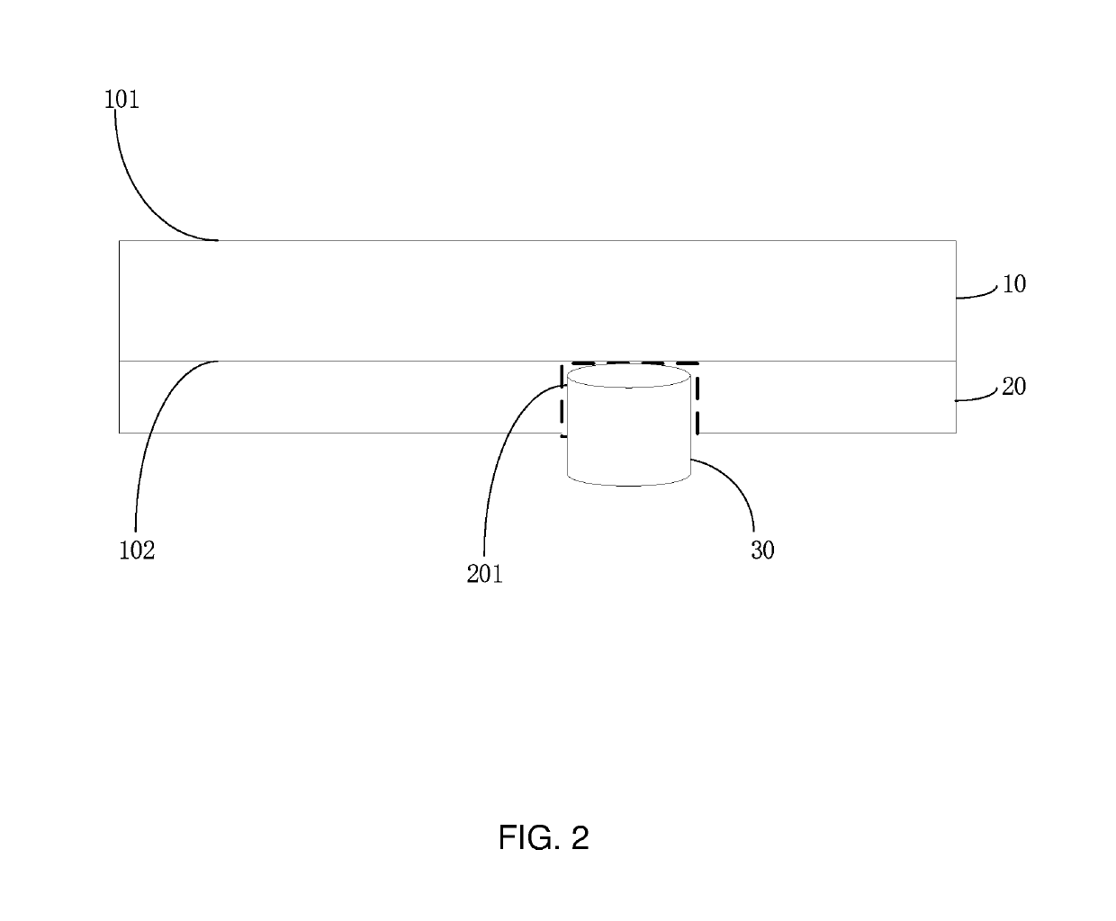
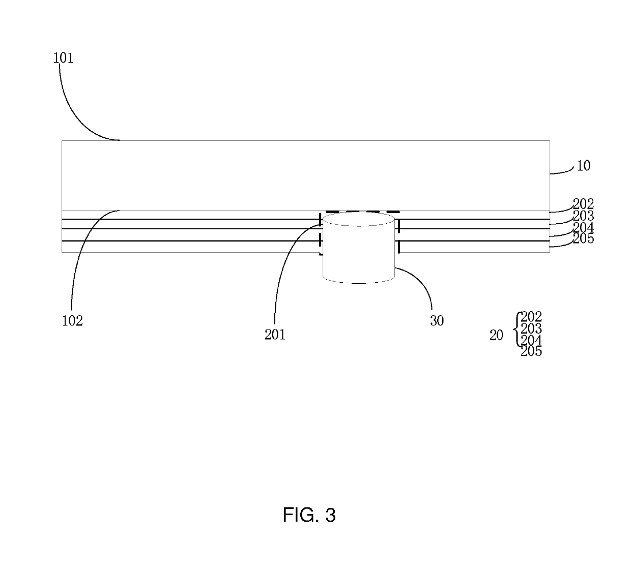
[0034]Please refer to FIGS. 1 to 2. FIG. 1 is a schematic view of a structure of a display device according to a preferred embodiment of this present invention. FIG. 2 is a cross-sectional view taken along line A-B of the display device of FIG. 1, according to an exemplary embodiment of this present ...


PUM


Abstract

The present invention provides a display device. The device is provided with an opening on a film structure on a back surface of a display panel, and a fingerprint recognition module is arranged in the opening, thereby reducing distance between the fingerprint recognition module and the back surface of the display panel, to improve fingerprint recognition accuracy. In addition, the fingerprint recognition module can also be located at any position in middle range of the display panel, and is not limited to the edge region at the bottom of the display panel, so as to improve a screen ratio of the display device.

Description

FIELD OF INVENTION[0001]This disclosure relates to a field of liquid crystal displays, and more particularly to a display device.BACKGROUND OF INVENTION[0002]Present, display devices such as mobile phones and tablets are mainly locked / unlocked by fingerprints. Modern fingerprint recognition mainly adopts capacitive sensing technology. Principle of fingerprint recognition is that, when a finger touches top of a fingerprint recognition module, it will turn on capacitive electrodes arrayed in the fingerprint recognition module. At the same time, protruding ridges of the finger make direct contact with the capacitive electrodes, and depressed valleys of the finger are far away from the capacitive electrodes, so that different sensing capacitance can be produced. Fingerprint information of a contact person will be obtained by converting the sensing capacitance into an image data, and hence the subsequent fingerprint comparison and identification operation can be executed.[0003]Prior art ...

Claims


Application Information

Patent Timeline
Patent Type & Authority Applications(United States)
IPC IPC(8): G06K9/00H01L27/32H01L51/52G06V40/13
CPCG06K9/00013H01L27/323H01L27/3234G06K9/0004H01L51/52H01L51/529G06K9/0002H01L27/3244G06V40/13H10K59/65H10K59/40H10K59/12H10K59/8794G06V40/1306G06V40/1318H10K50/80H10K50/87H10K59/00
Inventor YE, JIAN
Owner WUHAN CHINA STAR OPTOELECTRONICS SEMICON DISPLAY TECH CO LTD
Learn More