Pixel and organic light emitting display device having the same

a display device and organic light technology, applied in the field of display devices, can solve the problems of the threshold voltage of the driving transistor being relatively complex, the size of the display panel driver/pixel circuit may be large, etc., and achieve the effect of increasing the opening ratio of the display panel, reducing the number of signal lines, and increasing the size of the display panel driver/pixel circui

Inactive Publication Date: 2018-10-23
SAMSUNG DISPLAY CO LTD
View PDF3 Cites 6 Cited by
  • Summary
  • Abstract
  • Description
  • Claims
  • Application Information

AI Technical Summary

Benefits of technology

[0007]Example embodiments provide a pixel capable of increasing an opening ratio of the display panel.
[0008]Example embodiments provide an organic light emitting display device capable of decreasing a size of a display panel driver and reducing the power consumption.
[0029]Therefore, a pixel according to example embodiments compensates a threshold voltage of a driving transistor using scan signals and an emission control signal, thereby reducing the number of signal lines and increasing an opening ratio of the display panel.
[0030]An organic light emitting display device according to example embodiments uses previous scan signals as a voltage control signal and an initialization control signal, thereby decreasing a size of the display panel driver / pixel circuit and reducing the power consumption. In addition, the organic light emitting display device can reduce the number of signal lines in the display panel, thereby increasing the opening ratio of the display panel and improving the display quality.

Problems solved by technology

However, the pixels and / or the display panel driver (e.g., a scan driver, an emission control driver, etc) providing driving signals to the pixels for compensating the threshold voltage of the driving transistor may have a relatively complex structure.

Method used


Image

  • Pixel and organic light emitting display device having the same
  • Pixel and organic light emitting display device having the same
  • Pixel and organic light emitting display device having the same

Examples


Embodiment Construction

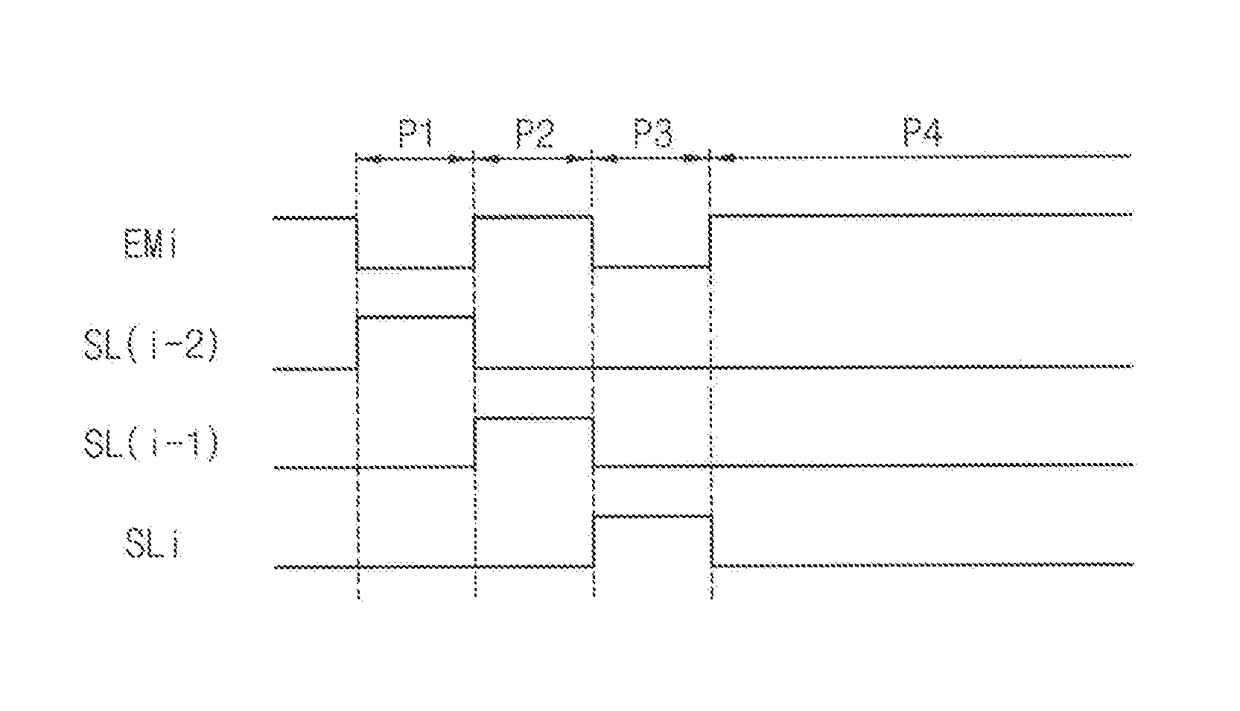
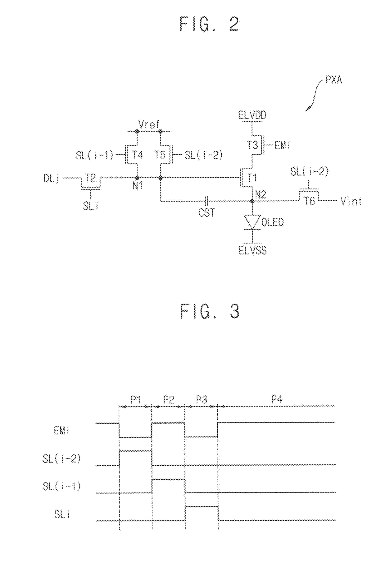
[0041]Exemplary embodiments will be described more fully hereinafter with reference to the accompanying drawings, in which various embodiments are shown.

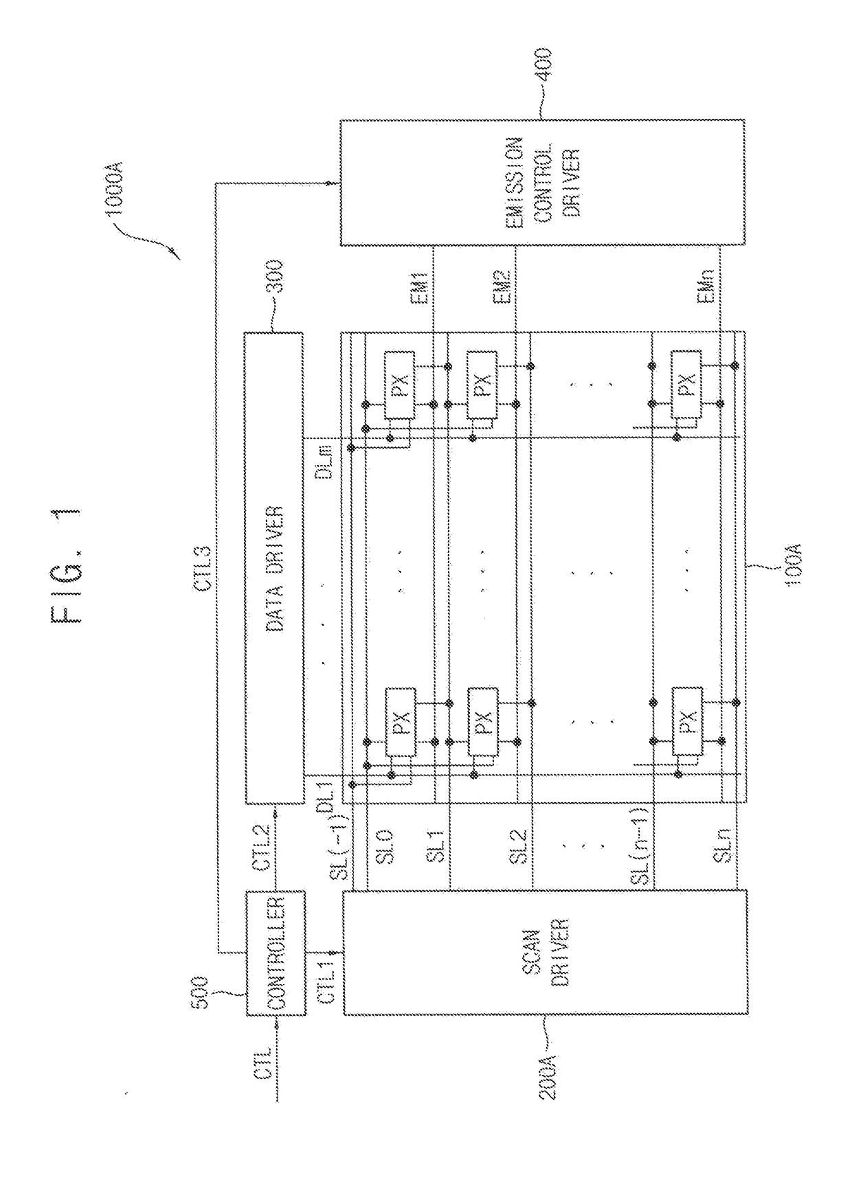
[0042]FIG. 1 is a block diagram illustrating an organic light emitting display device 1000A according to one example embodiment.

[0043]Referring to FIG. 1, the organic light emitting display device 1000A may include a display panel 100A, a scan driver 200A, a data driver 300, an emission control driver 400, and a controller 500.

[0044]The display panel 100A may include a plurality of pixels PX to display an image. For example, the display panel 100A may include n*m pixels PX because the pixels PX are arranged at locations corresponding to crossing points of scan lines SL1 through SLn and data lines DL1 through DLm.

[0045]Each pixel PX may receive a scan signal, a voltage control signal, an emission control signal, an initialization control signal, and a data signal and may emit the light based on the data signal. The pixels PX may rece...


PUM


Abstract

A pixel includes first through sixth transistors and an organic light emitting diode. The first transistor includes a gate electrode connected to a first node, a first electrode, and a second electrode connected to a second node. The second transistor provides a data signal to the first node in response to a scan signal. The third transistor provides a first power voltage to the first transistor in response to an emission control signal. The fourth transistor provides a reference voltage to the first node in response to a voltage control signal. The fifth transistor provides the reference voltage to the first node in response to an initialization control signal. The sixth transistor provides an initialization voltage to the second node in response to the initialization control signal. The organic light emitting diode is connected between the second node and a second power voltage.

Description

CROSS REFERENCE TO RELATED APPLICATION[0001]This application claims priority under 35 U.S.C. § 119 to Korean Patent Application No. 10-2016-0024631 filed on Feb. 29, 2016, the disclosure of which is hereby incorporated by reference herein in its entirety.BACKGROUND[0002]1. Technical Field[0003]Example embodiments of the inventive concept relate to display devices. More particularly, example embodiments of the inventive concept relate to a pixel and an organic light emitting display device having the pixel.[0004]2. Description of the Related Art[0005]An organic light emitting display device displays an image using organic light emitting diodes (OLEDs). The organic light emitting diodes includes an organic layer between two electrodes, namely, an anode and a cathode. The holes from the anode may be combined with the electrons from the cathode in the organic layer between the anode and the cathode to emit light.[0006]A deviation among the threshold voltages of driving transistors of pi...

Claims


Application Information

Patent Timeline
Patent Type & Authority Patents(United States)
IPC IPC(8): G06F3/038G09G3/3266G09G3/3233G09G3/3258G09G3/3275G09G5/00
CPCG09G3/3258G09G3/3233G09G3/3266G09G3/3275G09G2330/021G09G2300/0465G09G2300/0809G09G2300/0819G09G2300/0842G09G2300/0866G09G2310/0262G09G2310/0286G09G2310/08
Inventor PARK, KYOUNG-JINKIM, YONG-JAECHO, YOUNG-JINCHOI, DEOK-YOUNG
Owner SAMSUNG DISPLAY CO LTD
Why Eureka
Try Eureka