Photoelectric conversion element and solid-state imaging apparatus

a technology of conversion elements and conversion elements, applied in the direction of solid-state devices, radiation controlled devices, semiconductor devices, etc., can solve problems such as reducing sensitivity

Active Publication Date: 2019-07-25
SONY SEMICON SOLUTIONS CORP
View PDF0 Cites 1 Cited by
  • Summary
  • Abstract
  • Description
  • Claims
  • Application Information

AI Technical Summary

Benefits of technology

The patent aims to develop a photoelectric conversion element and a solid-state imaging apparatus that have excellent spectral shape, high responsivity, and high external quantum efficiency. This is achieved by using two organic semiconductor materials with mutually different mother skeletons. By using fullerene or its derivatives as a p-type semiconductor, the photoelectric conversion layer achieves high hole and electron mobility while maintaining a sharp spectral shape. This allows for better charge transport efficiency, resulting in a photoelectric conversion element with high responsivity and external quantum efficiency. The combination of these features results in a solid-state imaging apparatus with excellent color reproduction and sensitivity.

Problems solved by technology

In addition, in a case where a color filter including two-dimensionally arranged primary color filters of red, green, and blue is used for colorization, green light and blue light are absorbed by the color filter in a red pixel, for example, thus leading to the reduced sensitivity.

Method used


Image

  • Photoelectric conversion element and solid-state imaging apparatus
  • Photoelectric conversion element and solid-state imaging apparatus
  • Photoelectric conversion element and solid-state imaging apparatus

Examples


first embodiment (

1. First Embodiment (Example of a photoelectric conversion layer including three kinds of materials)

1-1. Configuration of Photoelectric Conversion Element

[0028]1-2. Method of Manufacturing Photoelectric conversion element

1-3. Workings and Effects

[0029]2. Second Embodiment (Example of photoelectric conversion layer including two kinds of materials)

application examples

3. Application Examples

4. Examples

1. First Embodiment

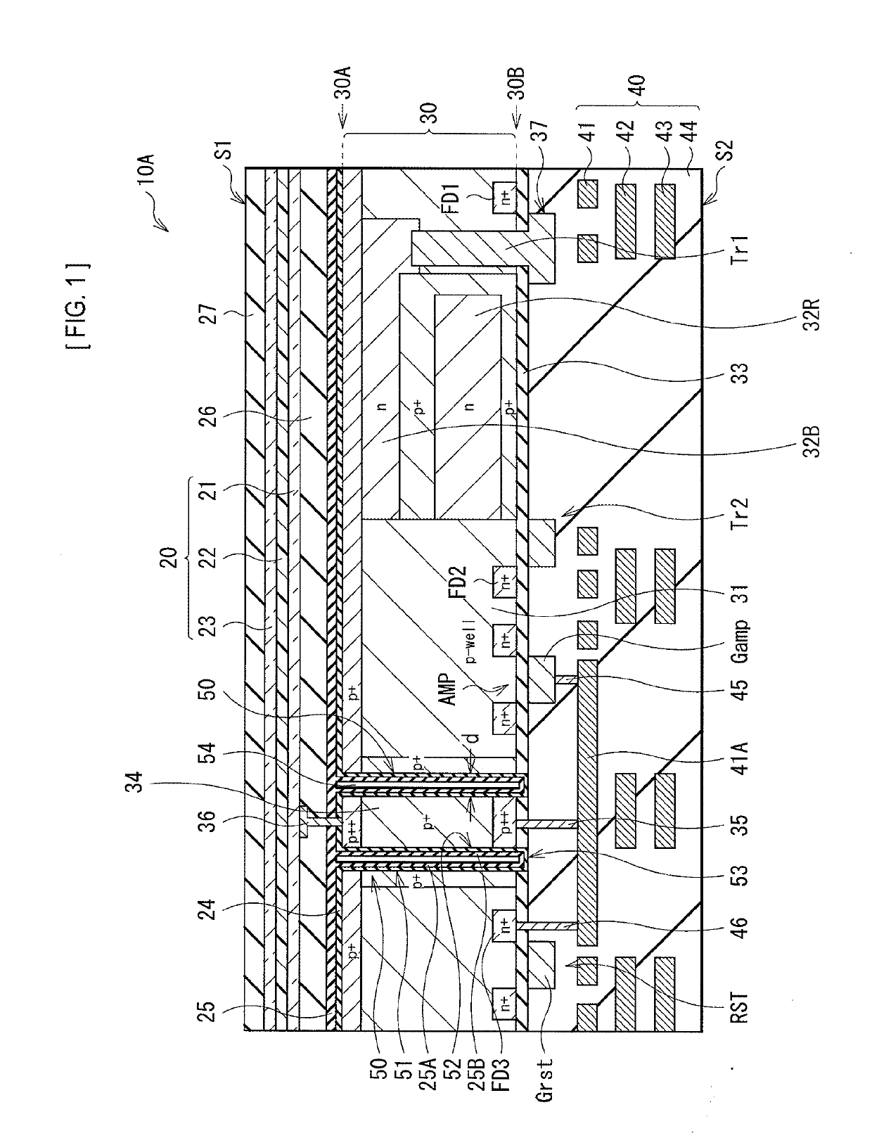
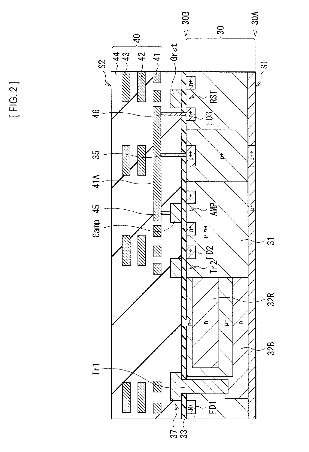
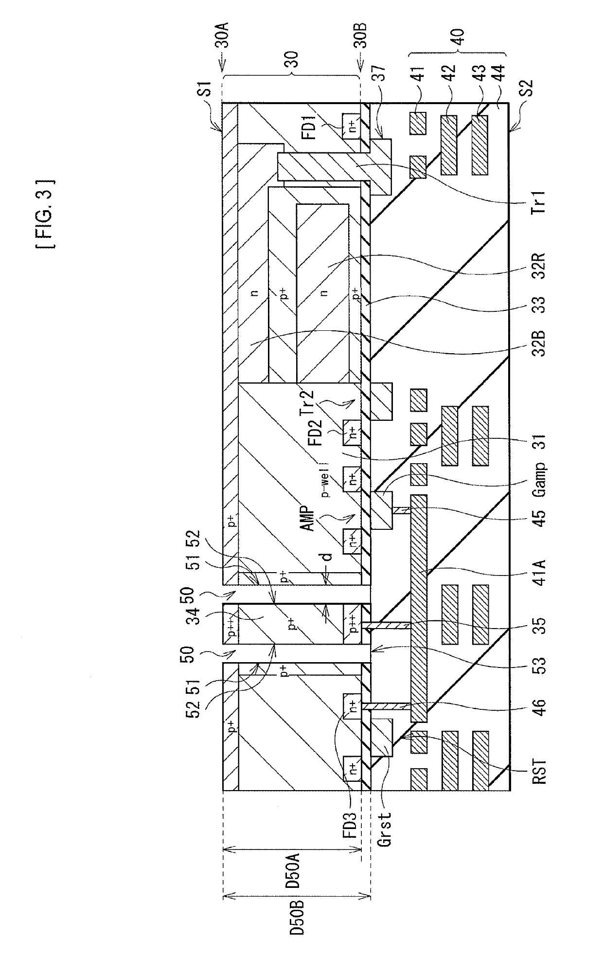
[0030]FIG. 1 illustrates a cross-sectional configuration of a photoelectric conversion element (a photoelectric conversion element 10A) according to a first embodiment of the present disclosure. The photoelectric conversion element 10A configures a pixel (a unit pixel P) in a solid-state imaging apparatus (a solid-state imaging apparatus 1: see FIG. 7) such as a CMOS image sensor used in an electronic apparatus such as a digital still camera, or a video camera, for example.

1-1. Configuration of Photoelectric Conversion Element

[0031]The photoelectric conversion element 10A is of a so-called longitudinal spectral type in which, for example, one organic photoelectric converter 20 and two inorganic photoelectric converters 32B and 32R are stacked in a longitudinal direction. The organic photoelectric converter 20 is provided on a side on which a first surface (back side) 30A is located of a semiconductor substrate 30. The inorganic ph...

second embodiment

2. Second Embodiment

[0108]FIG. 6 schematically illustrates a cross-sectional configuration of a photoelectric conversion element (a photoelectric conversion element 10B) of a second embodiment of the present disclosure. The photoelectric conversion element 10B is of a so-called longitudinal spectral type in which one organic photoelectric converter 60 and two inorganic photoelectric converters 32B and 32R are stacked in the longitudinal direction. The photoelectric conversion element 10B of the present embodiment differs from the foregoing first embodiment in that a photoelectric conversion layer 62 includes two kinds of organic semiconductor materials (the first organic semiconductor material and the second organic semiconductor material) that have mutually different mother skeletons. In the photoelectric conversion element 10B, the light entering the organic photoelectric converter 60 is absorbed by the second organic semiconductor material of the photoelectric conversion layer 62...


PUM


Abstract

A photoelectric conversion element according to an embodiment of the present disclosure includes a first electrode and a second electrode opposed to each other; and a photoelectric conversion layer provided between the first electrode and the second electrode, and including a first organic semiconductor material and a second semiconductor material that have mutually different mother skeletons, in which the first organic semiconductor material is fullerene or a fullerene derivative, and the second organic semiconductor material has a deeper HOMO level than the first organic semiconductor material.

Description

TECHNICAL FIELD[0001]The present disclosure relates to a photoelectric conversion element using an organic semiconductor material, for example, and a solid-state imaging apparatus including the same.BACKGROUND ART[0002]In recent years, in a solid-state imaging apparatus such as a CCD (Charge Coupled Device) image sensor or a CMOS (Complementary Metal Oxide Semiconductor) image sensor, miniaturization of pixel size has been under way. This causes a reduction in the number of photons entering a unit pixel, thus resulting in reduced sensitivity and a lower S / N ratio. In addition, in a case where a color filter including two-dimensionally arranged primary color filters of red, green, and blue is used for colorization, green light and blue light are absorbed by the color filter in a red pixel, for example, thus leading to the reduced sensitivity. Moreover, upon generation of a signal of each color, interpolation processing is performed between the pixels, thus generating a false color.[0...

Claims


Application Information

Patent Timeline
IPC IPC(8): H01L27/30H01L51/42H01L27/28
CPCH01L27/307H01L51/424H01L27/286H01L51/0078H01L51/0072H01L51/0046H01L51/0053H01L27/146H01L31/10Y02E10/549H10K85/211H10K85/215H10K85/6574H10K85/322H10K85/6572H10K30/30H10K39/32H10K39/10H10K30/00H10K19/20H10K30/20H10K30/451H10K39/00H10K85/311H10K85/621
Inventor MATSUZAWA, NOBUYUKIHASEGAWA, YUTAOBANA, YOSHIAKITAKEMURA, ICHIROYAMAGUCHI, TETSUJIENOKI, OSAMU
Owner SONY SEMICON SOLUTIONS CORP
Why Eureka
Try Eureka