Array substrate, display panel and pixel patching method

Active Publication Date: 2019-03-21
TCL CHINA STAR OPTOELECTRONICS TECH CO LTD
View PDF9 Cites 3 Cited by
  • Summary
  • Abstract
  • Description
  • Claims
  • Application Information

AI Technical Summary

Benefits of technology

The present invention provides an array substrate, a display panel, and a pixel patching method that can improve the sensory experience after patch. By disconnecting the data line and input terminal of an abnormal pixel region and conducting the first and second contacts with a conductive member, the potential of the pixel electrode of the abnormal region is made the same as that of its adjacent normal region, enabling the abnormal region to display the image of its adjacent normal region. This improves the sensory experience after the pixel is repaired, avoids waste of subsequent targets, and increases product yield.

Problems solved by technology

Making an array substrate of a LCD panel is a relative complicated process; a pattern is formed on a glass substrate by continuously repeating evaporation, exposure, development and etching for different film layers on the glass substrate.
The array substrate is generally easily has problems than the color filter substrate, due to the more processes required and the complexity and many processes has high demands on the environment.
There are usually particles, broken lines, short lines, etc. that can cause problems with the array.
Since the repaired liquid crystal display panel always has a dark point in one position, the sensory experience of the client when viewed will be affected.
The problem caused by this dark point repair will be more obvious when two consecutive pixels are performed with dark point repair.

Method used


Image

  • Array substrate, display panel and pixel patching method
  • Array substrate, display panel and pixel patching method
  • Array substrate, display panel and pixel patching method

Examples


Embodiment Construction

[0035]The technical solution in the embodiments of the present invention will be clearly and completely described below with reference to the accompanying drawings in the embodiments of the present invention. Apparently, the described embodiments are merely some but not all of the embodiments of the present invention. All other embodiments obtained by persons of ordinary skill in the art based on the embodiments of the present invention without creative efforts shall fall within the protection scope of the present invention.

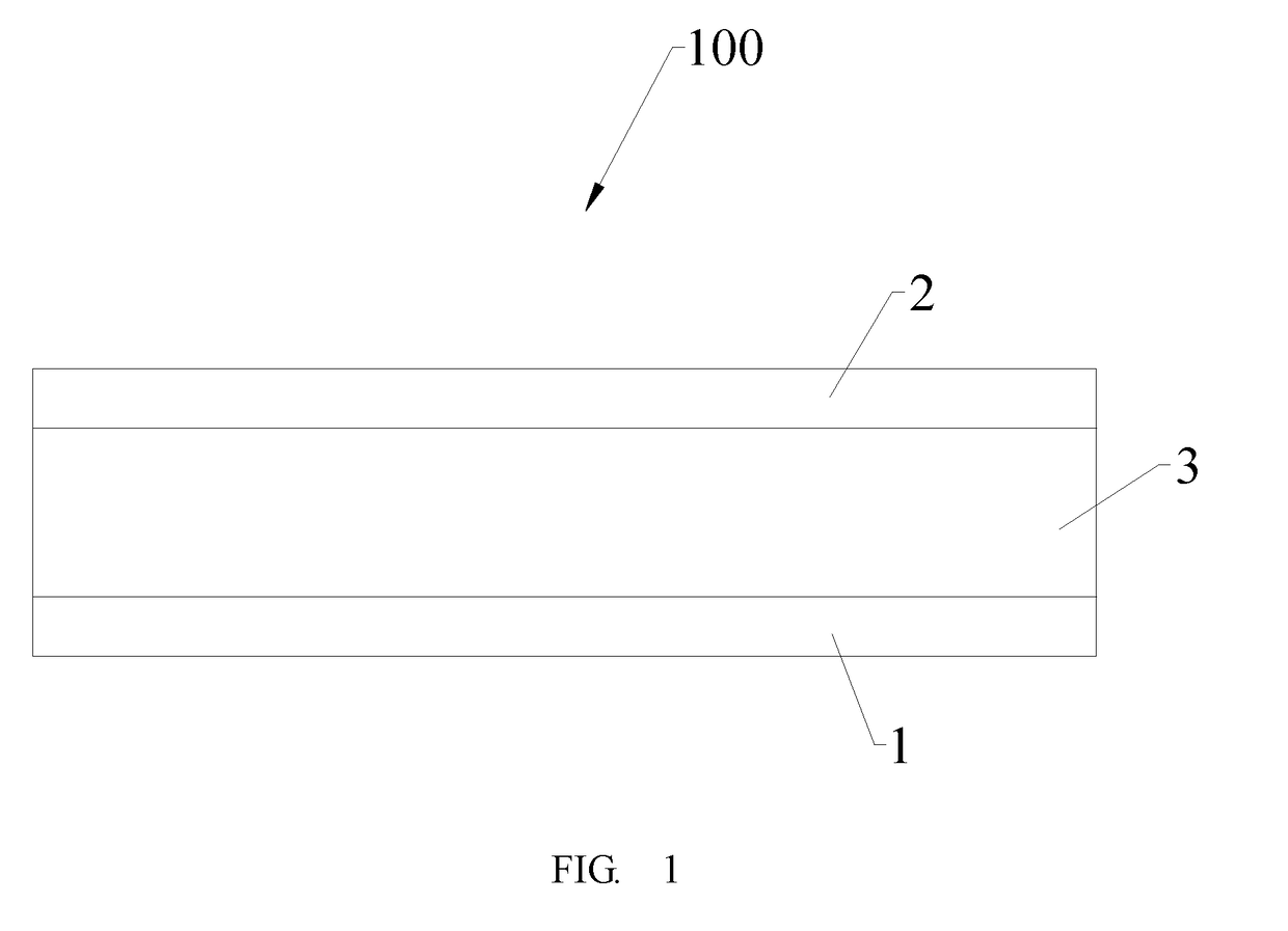
[0036]Please refer to FIG. 1 to FIG. 6, an embodiment of the present invention provides a display panel 100. The display panel 100 comprises an array substrate 1. The display panel 100 is applicable to various display devices. The display panel 100 further comprises a color filter (CF) substrate 2 disposed opposite to the array substrate 1, and a liquid crystal (LC) layer 3 disposed between the array substrate 1 and the CF substrate 2.

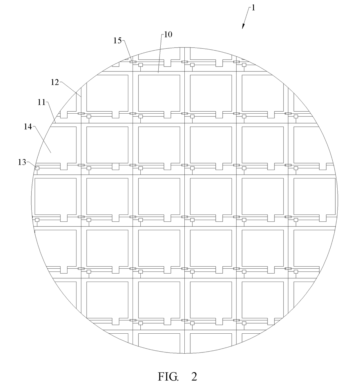
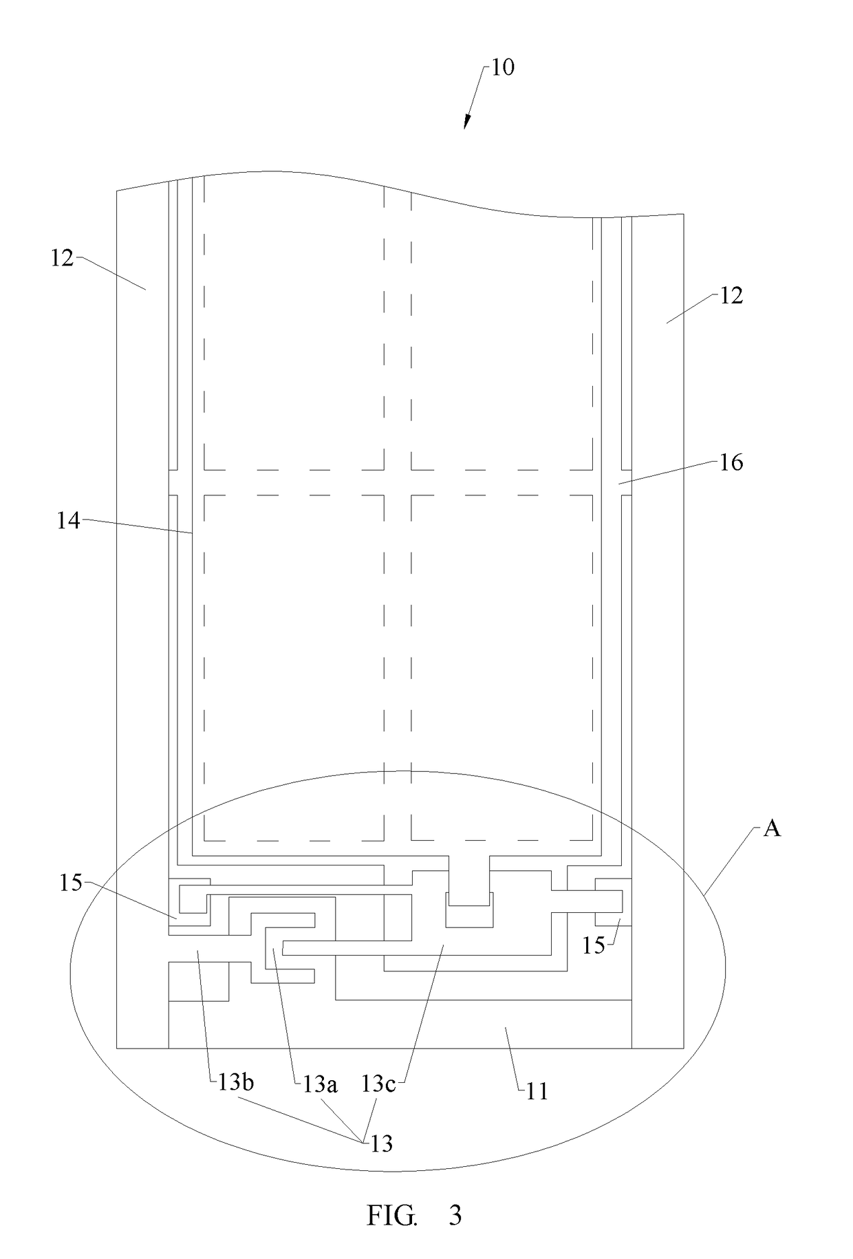
[0037]The array substrate 1 ...


PUM


Abstract

The present application provides an array substrate, which comprises a plurality of gate lines, a plurality of data lines, a plurality of thin film transistors, a plurality of pixel electrodes, and a plurality of conductive members. In each of the pixel regions, a control terminal of the TFT is electrically connected with the gate line, an input terminal of the TFT is electrically connected with the data line, and an output terminal of the TFT is electrically connected with the pixel electrode. The output terminal comprises a body, and a first contact and a second contact which are connected with the body. The first contact and one of the conductive members extending into the pixel region are overlapping-disposed and insulated from each other. The second contact and another of the conductive members extending into the pixel region are overlapping-disposed and insulated from each other.

Description

BACKGROUND OF THE APPLICATION[0001]This application claims the priority of an application No. 201710858164.1 filed on Sep. 20, 2017, entitled “ARRAY SUBSTRATE, DISPLAY PANEL AND PIXEL PATCHING METHOD”, the contents of which are hereby incorporated by reference.FIELD OF APPLICATION[0002]The present disclosure relates to the field of liquid crystal display technology, and particularly to an array substrate, a display panel and a pixel patching method.DESCRIPTION OF PRIOR ART[0003]With development of display technology, flat panel display devices such as liquid crystal displays (LCDs) are widely used in mobile phones, televisions, personal digital assistants (PDAs), digital cameras, laptops, desktop computers and other consumer electronics products, because of their advantages of high image quality, low power consumption, thin body and wide application range, and have become the mainstream of display devices.[0004]Most liquid crystal display devices on the market are backlight type LCD...

Claims


Application Information

Patent Timeline
IPC IPC(8): H01L27/12G02F1/1362G02F1/1368
CPCH01L27/124G02F1/136259G02F1/1368G02F1/136213G02F1/136286G02F2201/121G02F2201/123
Inventor AN, LIYANG
Owner TCL CHINA STAR OPTOELECTRONICS TECH CO LTD
Why Eureka
Try Eureka