
Antenna device having slit structure and electronic device including the same

Active Publication Date: 2018-09-20
SAMSUNG ELECTRONICS CO LTD
View PDF0 Cites 23 Cited by
  • Summary
  • Abstract
  • Description
  • Claims
  • Application Information

AI Technical Summary

Benefits of technology

The present invention provides an antenna device and an electronic device with the antenna device that have a slit structure. This structure prevents degradation of the antenna device performance even if the housing of the electronic device is made using a metallic member. Additionally, the slit structure reduces degradation of the antenna device performance when the electronic device is gripped.

Problems solved by technology

However, electronic devices have a limited volume of space for an antenna.
It is difficult to satisfy a provider's specification and an electromagnetic wave absorption rate (specific absorption rate (SAR)) standard or to minimize an effect on a human body while implementing the above-mentioned bands in one antenna device.
However, an antenna device using a slit (e.g., a board slit) in a PCB and a non-conductive slit in a housing may control one frequency operating band according to the length of the slit, but may not operate in multiple frequency bands.
In addition, when a plurality of antenna power-feeding portions is added in order to form multi-band resonance, an isolation issue may occur between antennas using a slit as a radiator, so that radiation performance may deteriorate.
In addition, an antenna device, which operates using a non-conductive slit extending across both ends in a width direction of an electronic device and a slit in the PCB, may be degraded in radiation performance when the electronic device is gripped (e.g., a hand effect).

Method used


Image

  • Antenna device having slit structure and electronic device including the same
  • Antenna device having slit structure and electronic device including the same
  • Antenna device having slit structure and electronic device including the same

Examples


example electronic

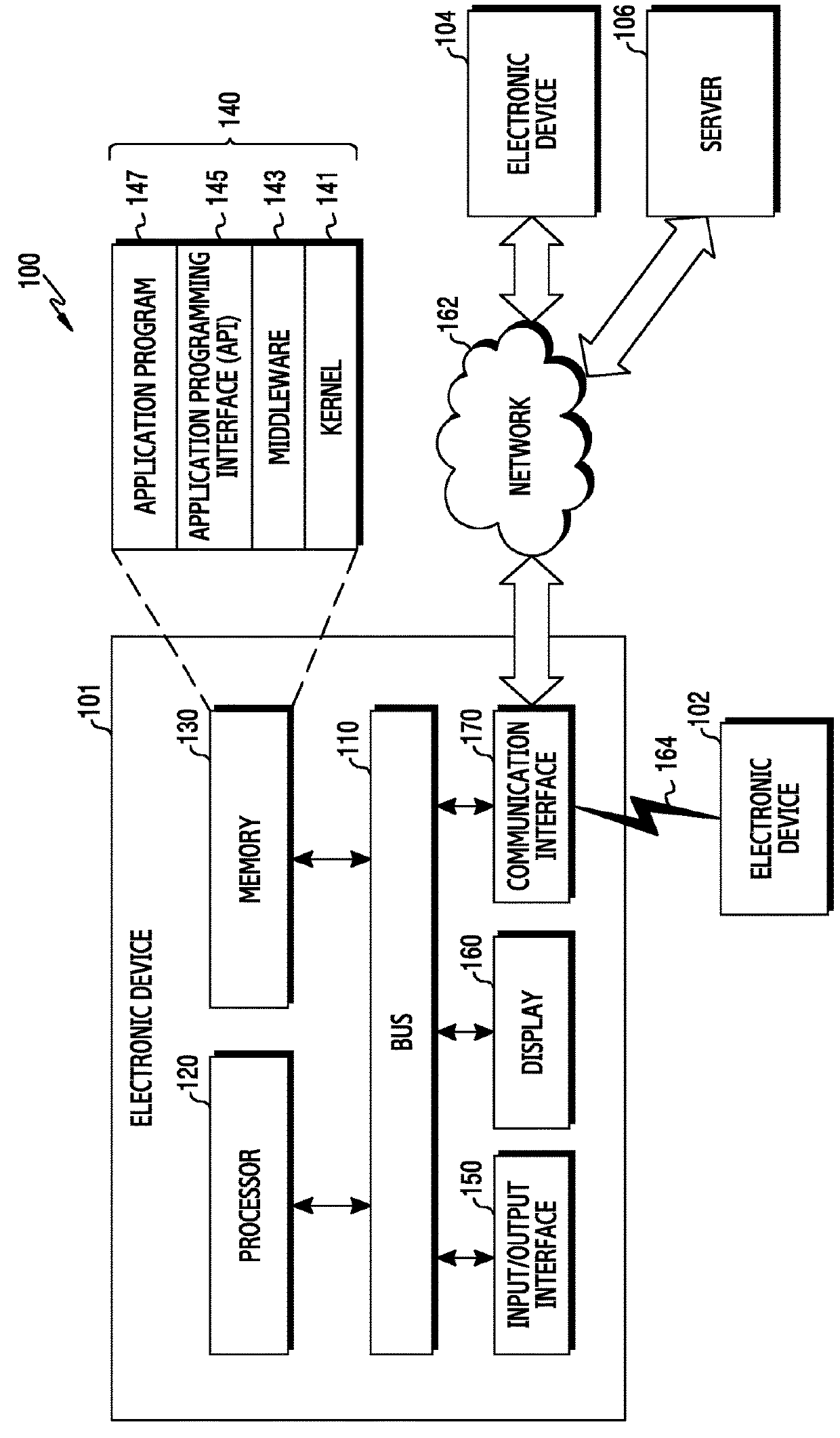
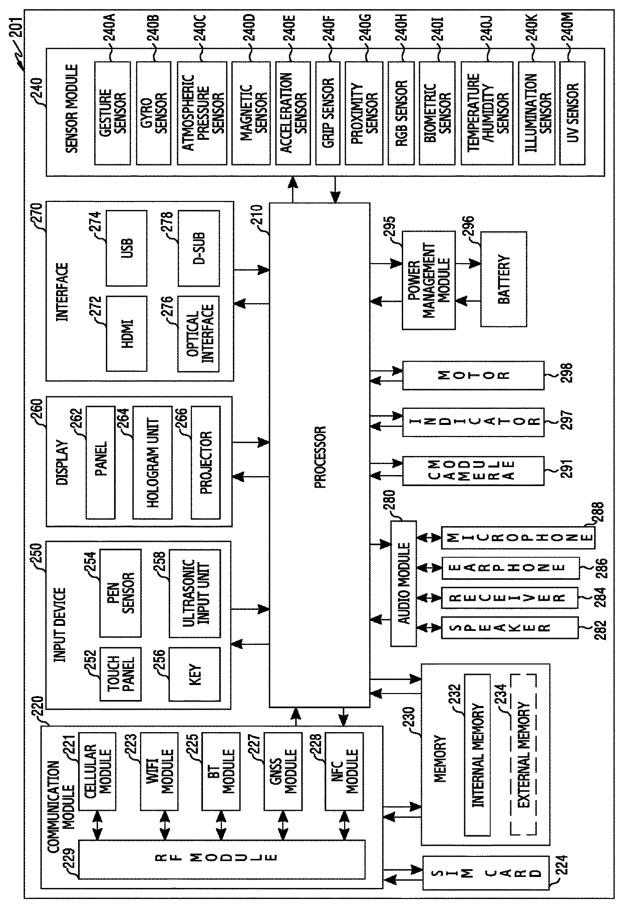
[0052 devices may include smart phones, tablet personal computers (PCs), mobile phones, video telephones, electronic book readers, desktop PCs, laptop PCs, netbook computers, workstations, servers, personal digital assistants (PDAs), portable multimedia players (PMPs), motion picture experts group (MPEG-1 or MPEG-2) audio layer 3 (MP3) players, mobile medical devices, cameras, and / or wearable devices, or the like, but are not limited thereto. For example, wearable devices may include accessory-type wearable devices (e.g., watches, rings, bracelets, anklets, necklaces, glasses, contact lenses, or head-mounted-devices (HMDs)), fabric or clothing integral wearable devices (e.g., electronic clothes), body-mounted wearable devices (e.g., skin pads or tattoos), and / or implantable wearable devices (e.g., implantable circuits), or the like but are not limited thereto.

[0053]Electronic devices may include smart home appliances, such as televisions (TVs), digital versatile disk (DVD) players, ...


PUM


Abstract

An electronic device includes housing including first plate, second plate, and side member, wherein side member includes first side face in first direction having first length, second side face having second length greater than first length, third side face extending parallel to first side face having first length, and fourth side face; touch screen display disposed within housing, and exposed through portion of first plate; a PCB between first plate and second plate to be parallel to second plate, wherein PCB includes ground plane and first L-shaped ground extension between first conductive region of second plate and first plate, and first L-shaped ground extension includes first portion extending in second direction from ground plane and second portion extending in first direction from first portion; and at least one first wireless communication circuit disposed on PCB and electrically connected to first point in second portion of first L-shaped ground extension.

Description

CROSS-REFERENCE TO RELATED APPLICATION(S)[0001]This application is based on and claims priority under 35 U.S.C. § 119 to Korean Patent Application No. 10-2017-0032324, filed on Mar. 15, 2017, in the Korean Intellectual Property Office, the disclosure of which is incorporated by reference herein in its entirety.BACKGROUND[0002]1) Field[0003]The present disclosure relates generally to an antenna device having a slit structure and an electronic device including the same and, more particularly, to an antenna device and an electronic device having the antenna device, in which the antenna device has a slit structure, which is implemented to be capable of operating in multi-bands in the antenna device, which uses a non-conductive slit formed in a housing and a slit formed in a printed circuit board (PCB).[0004]2) Description of Related Art[0005]The above information is presented as background information only to assist with an understanding of the present disclosure. No determination has b...

Claims


Application Information

Patent Timeline
IPC IPC(8): H01Q1/24H01Q1/08H01Q1/36H01Q1/44H03K17/96
CPCH01Q1/243H01Q1/085H01Q1/36H01Q1/44H03K17/96H01Q5/28H01Q5/307H01Q5/321H01Q5/35H01Q1/22H01Q1/50H05K5/0247H01Q13/10H01Q21/30H01Q1/48H01Q1/242H04M1/0249H04M1/0277H04M1/0274H01Q1/38H04M2250/06
Inventor KIM, JAEHYUNGHAN, SANG-MINKO, KYUNG-BAEKIM, YOUNGJUNGKIM, JONG-SUKKIM, TAEGYUBANG, JINKYUYU, CHANGHALEE, YOUNG-SUNG
Owner SAMSUNG ELECTRONICS CO LTD
Learn More