Goa circuit

Active Publication Date: 2018-08-02
WUHAN CHINA STAR OPTOELECTRONICS TECH CO LTD
View PDF3 Cites 7 Cited by
  • Summary
  • Abstract
  • Description
  • Claims
  • Application Information

AI Technical Summary

Benefits of technology

The present invention provides a GOA circuit that can achieve forward and backward scanning without using complicated control signals. This allows for a narrower border design and simplifies the driving timing, reducing the cost of ICs. Additionally, the circuit improves the current leakage at a specific node and ensures circuit stability.

Problems solved by technology

This approach requires the integrated circuit (IC) to provide the function to output the signals, which restricts the choice for the IC.
Moreover, because the co-existence of U2D and D2U, the layout also imposes restrictions on the narrow border design, and a higher IC cost will incur.

Method used


Image

  • Goa circuit
  • Goa circuit
  • Goa circuit

Examples


Embodiment Construction

[0066]To further explain the technical means and effect of the present invention, the following refers to embodiments and drawings for detailed description.

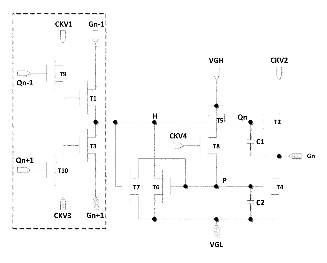
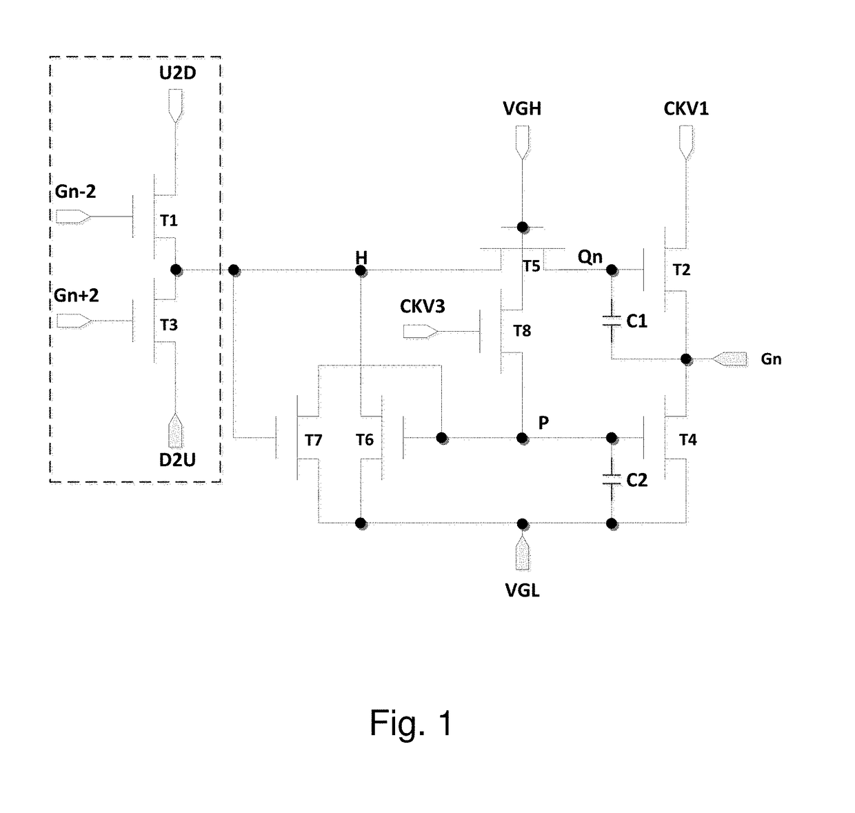
[0067]Refer to FIG. 4. The present invention provides a GOA circuit, applicable to an LTPS panel. The GOA circuit comprises: a plurality of cascade GOA units, for a positive integer n, the n-th GOA unit comprising: a first thin film transistor (TFT) T1, having a gate connected to a first source / drain of a ninth TFT T9, when n-th GOA unit not the first GOA unit in the cascade, a source and a drain of the first TFT T1 connected respectively to a signal output node Gn-1 of (n−1)-th GOA unit and a first node H; a second TFT T2, having a gate connected to a second node Qn of n-th GOA unit, a source and ae drain connected respectively to the signal output node Gn of n-th GOA unit and a second clock signal CKV2; a third TFT T3, when n-th GOA unit not the last GOA unit in the cascade, having a gate connected to a first source / drain of a ...


PUM


Abstract

The invention provides a GOA circuit, comprising a plurality of GOA units, for a positive integer n, n-th GOA unit comprising: a first TFT (T1), a second TFT (T2), a third TFT (T3), a fourth TFT T(4), a fifth TFT (T5), a sixth TFT (T6), a seventh TFT (T7), an eighth TFT (T8), a ninth TFT (T9), a tenth TFT (T10), a first capacitor (C1) and a second capacitor (T2). The invention, based on known GOA circuit, uses T9 and T10 so as to achieve forward and backward scanning without D2U and U2D control signals, which facilitates narrow border design and simplifies corresponding driving timing and reduce IC cost. The pre-charging unit formed by T1, T9, T3, and T10 effectively improves the current leakage and ensures GOA circuit stability.

Description

BACKGROUND OF THE INVENTION1. Field of the Invention[0001]The present invention relates to the field of display, and in particular to a gate driver on array (GOA) circuit.2. The Related Arts[0002]The gate driver on array (GOA) technology is the array substrate column drive technology, by using the array substrate process for the LCD panel to manufacture the driver circuit for the gate scan line on the array substrate to achieve driving of the gates by line-by-line scanning.[0003]The GOA circuit must provide the forward and backward scanning function. The common approach is to add a U2D and a D2U scanning units. For forward scanning, the forward scanning control signal U2D is high voltage, and the backward scanning control signal is low voltage. This approach requires the integrated circuit (IC) to provide the function to output the signals, which restricts the choice for the IC. Moreover, because the co-existence of U2D and D2U, the layout also imposes restrictions on the narrow bor...

Claims


Application Information

Patent Timeline
IPC IPC(8): G09G3/3266G09G3/36G09G3/3258
CPCG09G3/3266G09G3/3677G09G3/3258G09G3/3648G09G3/3696G09G2310/0283G09G2310/08G09G2320/0214G09G2300/0408G11C19/184G11C19/28
Inventor LI, YAFENG
Owner WUHAN CHINA STAR OPTOELECTRONICS TECH CO LTD
Why Eureka
Try Eureka