Pressure contact-type semiconductor module

Active Publication Date: 2018-06-21
FUJI ELECTRIC CO LTD
View PDF6 Cites 0 Cited by
  • Summary
  • Abstract
  • Description
  • Claims
  • Application Information

AI Technical Summary

Benefits of technology

The present invention aims to provide a pressure contact-type semiconductor module that can accurately adjust the pressure contact-receiving surfaces of the plural semiconductor units to be on the same plane, resulting in uniform pressure application without any localized high pressure contact force applied on each semiconductor unit and reducing the pressure contact load. The invention includes a plurality of semiconductor units disposed side-by-side, each containing a semiconductor device substrate, electrodes, and a pressure contact adjustment member with a top surface as a pressure contact-receiving surface to which a lead-out electrode plate that is common to the plural semiconductor units is to be pressure-contacted. The pressure contact adjustment members are screwed into the corresponding electrode plates such that levels of their top surfaces are adjustable to match a reference pressure contact plane.

Problems solved by technology

However, in the pressure contact-type power semiconductor module disclosed in Patent Document 2, the three solder plates are melted and solidified in a pressurized state, which poses the unsolved problem that it is difficult to have a precisely uniform thickness for the entirety of the semiconductor chips, multiple solder plates, and the heat cushioning plates, and to apply more uniform pressure.
Furthermore, in the pressure contact-type power semiconductor module disclosed in Patent Document 3, the columnar electrode parts are plastically deformed, which poses the unsolved problem that localized stress is applied to the surface of the electrodes of the semiconductor chips.

Method used


Image

  • Pressure contact-type semiconductor module
  • Pressure contact-type semiconductor module
  • Pressure contact-type semiconductor module

Examples


embodiment 1

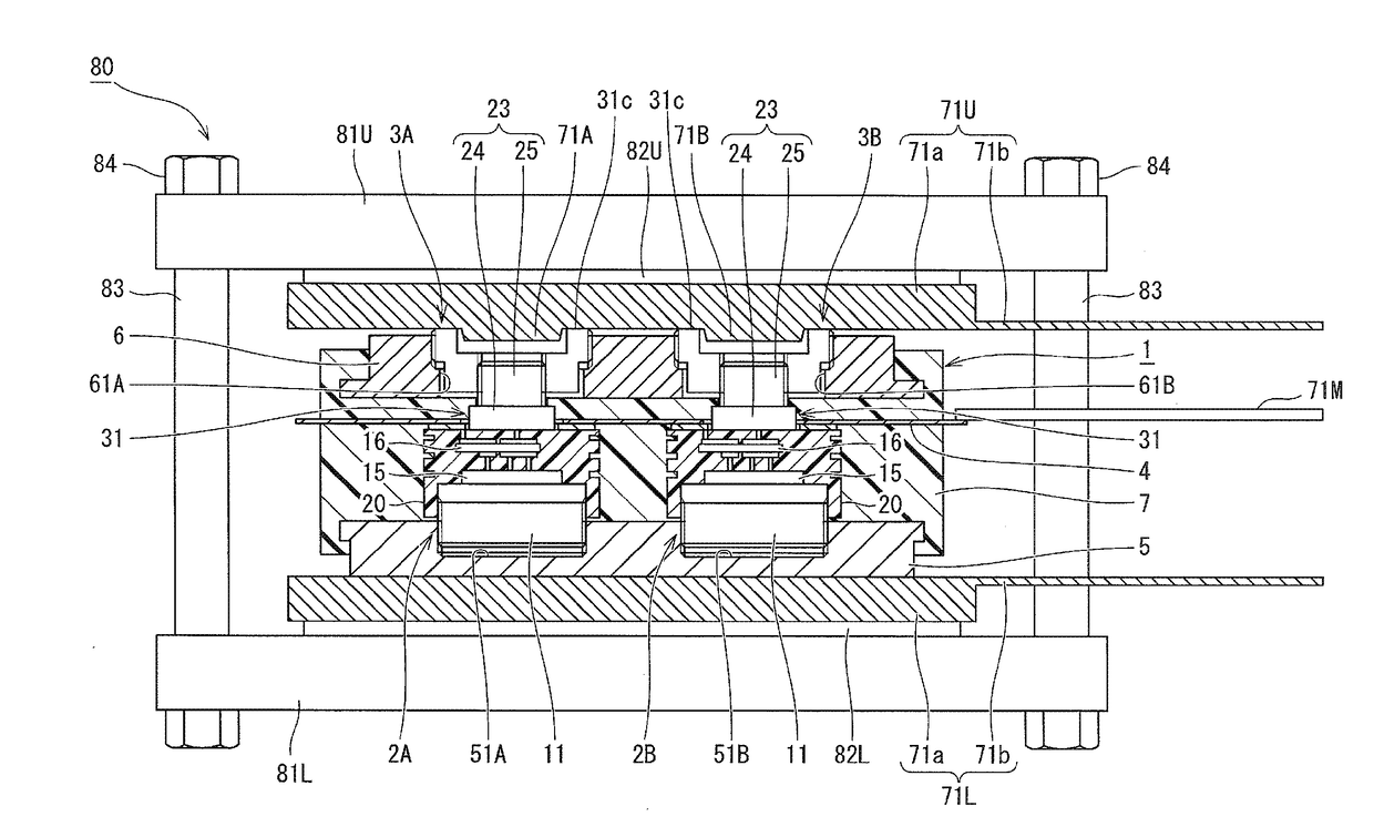
[0026]Below, Embodiment 1 of a pressure contact-type semiconductor module according to the present invention will be described with reference to drawings.

[0027]As shown in FIG. 1, the pressure contact-type semiconductor module of the present invention includes a semiconductor device 1, and an external pressure contact mechanism 80 that is in pressure contact with the semiconductor device 1.

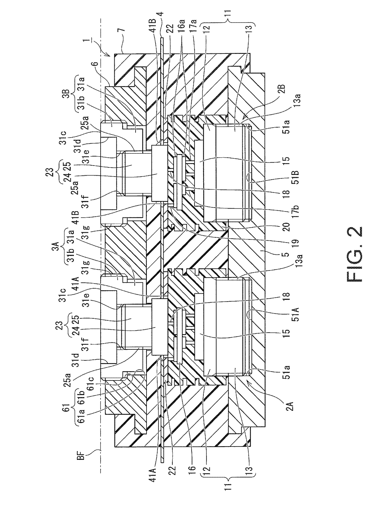
[0028]As shown in FIG. 2, for example, the semiconductor device 1 includes two semiconductor units 2A and 2B having the same configuration, pressure contact adjustment members 3A and 3B, a control electrode plate 4, a first pressure contact electrode plate 5, a second pressure contact electrode plate 6, and a resin sealing material 7.

[0029]

[0030]As shown in FIGS. 2 and 3, the semiconductor units 2A and 2B each have a base substrate 11. The base substrate 11 includes a wiring pattern plate 12 made of relatively thick copper, and a first electrode 13 similarly made of copper that is formed on the bo...


PUM


Abstract

A pressure contact-type semiconductor module includes a plurality of semiconductor units disposed side-by-side, each of the semiconductor units including: a semiconductor device substrate; a first electrode formed below the semiconductor device substrate, a second electrode formed above the semiconductor device substrate, an electrode plate electrically connected to the second electrode; and a pressure contact adjustment member screwed into the electrode plate, the pressure contact adjustment member having a top surface as a pressure contact-receiving surface to which a lead-out electrode plate that is common to the plurality of semiconductor units is to be pressure-contacted, levels of the respective top surfaces of the pressure contact adjustment members in the plurality of semiconductor units being adjustable to match a reference pressure contact plane so that contact pressures in the respective top surfaces applied by the lead-out electrode plate are substantially the same among the semiconductor units.

Description

BACKGROUND OF THE INVENTIONTechnical Field[0001]The present invention relates to a pressure contact-type semiconductor module equipped with a power semiconductor chip.Background Art[0002]Power semiconductor modules are used in inverter devices, uninterruptible power supplies, machine tools, industrial robots, and the like.[0003]One known example of a conventional power semiconductor module is disclosed in Patent Document 1, for example.[0004]The power semiconductor module disclosed in Patent Document 1 includes a support plate having a plurality of penetrating holes that pass through both the first surface and second surface, which are opposite to each other, and a plurality of semiconductor units that are fixed to the first surface of the support plate and that have semiconductor chips and protruding metal blocks, the metal blocks passing through the penetrating holes to the second surface. The semiconductor units include connecting terminals that protrude in a direction opposite t...

Claims


Application Information

Patent Timeline
IPC IPC(8): H01L25/07H01L23/32H01L23/492
CPCH01L25/072H01L23/32H01L23/492H01L25/115H01L24/72H01L2924/181H01L2924/1815H01L2224/01H01L2924/00012
Inventor IIZUKA, YUJI
Owner FUJI ELECTRIC CO LTD
Why Eureka
Try Eureka